CY8C27x43 Final Data Sheet
3. Electrical Specifications
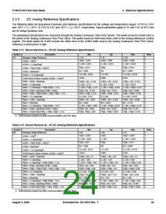
3.3.6
DC Analog Reference Specifications
The following tables list guaranteed maximum and minimum specifications for the voltage and temperature ranges: 4.75V to 5.25V
and -40°C ≤ TA ≤ 85°C, or 3.0V to 3.6V and -40°C ≤ TA ≤ 85°C, respectively. Typical parameters apply to 5V and 3.3V at 25°C and
are for design guidance only.
The guaranteed specifications are measured through the Analog Continuous Time PSoC blocks. The power levels for AGND refer to
the power of the Analog Continuous Time PSoC block. The power levels for RefHi and RefLo refer to the Analog Reference Control
register. The limits stated for AGND include the offset error of the AGND buffer local to the Analog Continuous Time PSoC block.
Reference control power is high.
Table 3-11. Silicon Revision A – 5V DC Analog Reference Specifications
Symbol
Description
Bandgap Voltage Reference
Min
Typ
Max
Units
BG
–
1.274
1.30
1.326
V
V
AGND = Vdd/2a
Vdd/2 - 0.030
2 x BG - 0.043
P2[4] - 0.013
BG - 0.009
Vdd/2 - 0.004
2 x BG - 0.010
P2[4]
Vdd/2 + 0.003
2 x BG + 0.024
P2[4] + 0.014
BG + 0.009
AGND = 2 x BandGapa
AGND = P2[4] (P2[4] = Vdd/2)a
AGND = BandGapa
–
–
–
–
–
–
V
V
V
V
V
V
BG
AGND = 1.6 x BandGapa
1.6 x BG - 0.018
-0.034
1.6 x BG
0.000
1.6 x BG + 0.018
0.034
AGND Block to Block Variation (AGND = Vdd/2)a
RefHi = Vdd/2 + BandGap
Vdd/2 + BG - 0.140
3 x BG - 0.112
Vdd/2 + BG - 0.018
3 x BG - 0.018
Vdd/2 + BG + 0.103
3 x BG + 0.076
–
–
–
–
–
–
RefHi = 3 x BandGap
V
V
V
V
V
V
RefHi = 2 x BandGap + P2[6] (P2[6] = 1.3V)
RefHi = P2[4] + BandGap (P2[4] = Vdd/2)
RefHi = P2[4] + P2[6] (P2[4] = Vdd/2, P2[6] = 1.3V)
RefHi = 3.2 x BandGap
2 x BG + P2[6] - 0.113
P2[4] + BG - 0.130
P2[4] + P2[6] - 0.133
3.2 x BG - 0.112
2 x BG + P2[6] - 0.018
P2[4] + BG - 0.016
P2[4] + P2[6] - 0.016
3.2 x BG
2 x BG + P2[6] + 0.077
P2[4] + BG + 0.098
P2[4] + P2[6] + 0.100
3.2 x BG + 0.076
RefLo = Vdd/2 – BandGap
Vdd/2 - BG - 0.051
BG - 0.082
Vdd/2 - BG + 0.024
BG + 0.023
Vdd/2 - BG + 0.098
BG + 0.129
–
–
–
–
RefLo = BandGap
V
V
V
V
RefLo = 2 x BandGap - P2[6] (P2[6] = 1.3V)
RefLo = P2[4] – BandGap (P2[4] = Vdd/2)
RefLo = P2[4]-P2[6] (P2[4] = Vdd/2, P2[6] = 1.3V)
2 x BG - P2[6] - 0.084
P2[4] - BG - 0.056
P2[4] - P2[6] - 0.057
2 x BG - P2[6] + 0.025
P2[4] - BG + 0.026
P2[4] - P2[6] + 0.026
2 x BG - P2[6] + 0.134
P2[4] - BG + 0.107
P2[4] - P2[6] + 0.110
a. AGND tolerance includes the offsets of the local buffer in the PSoC block.
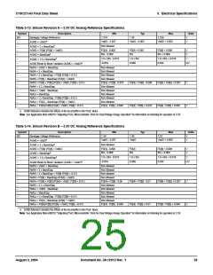
Table 3-12. Silicon Revision B – 5V DC Analog Reference Specifications
Symbol
Description
Bandgap Voltage Reference
Min
Typ
1.30
Max
1.32
Units
BG
–
1.28
V
V
AGND = Vdd/2a
Vdd/2 - 0.030
2 x BG - 0.043
P2[4] - 0.011
BG - 0.009
Vdd/2
Vdd/2 + 0.007
AGND = 2 x BandGapa
AGND = P2[4] (P2[4] = Vdd/2)a
AGND = BandGapa
–
–
–
–
–
–
2 x BG
P2[4]
2 x BG + 0.024
P2[4] + 0.011
BG + 0.009
1.6 x BG + 0.018
0.034
V
V
V
V
V
V
BG
AGND = 1.6 x BandGapa
1.6 x BG - 0.018
-0.034
1.6 x BG
0.000
AGND Block to Block Variation (AGND = Vdd/2)a
RefHi = Vdd/2 + BandGap
Vdd/2 + BG - 0.1
3 x BG - 0.06
Vdd/2 + BG - 0.01
3 x BG - 0.01
Vdd/2 + BG + 0.1
3 x BG + 0.06
–
–
–
–
–
–
RefHi = 3 x BandGap
V
V
V
V
V
V
RefHi = 2 x BandGap + P2[6] (P2[6] = 1.3V)
RefHi = P2[4] + BandGap (P2[4] = Vdd/2)
RefHi = P2[4] + P2[6] (P2[4] = Vdd/2, P2[6] = 1.3V)
RefHi = 3.2 x BandGap
2 x BG + P2[6] - 0.06
P2[4] + BG - 0.06
P2[4] + P2[6] - 0.06
3.2 x BG - 0.06
2 x BG + P2[6] - 0.01
P2[4] + BG - 0.01
P2[4] + P2[6] - 0.01
3.2 x BG - 0.01
2 x BG + P2[6] + 0.06
P2[4] + BG + 0.06
P2[4] + P2[6] + 0.06
3.2 x BG + 0.06
RefLo = Vdd/2 – BandGap
Vdd/2 - BG - 0.051
BG - 0.06
Vdd/2 - BG + 0.01
BG + 0.01
Vdd/2 - BG + 0.06
BG + 0.06
–
–
–
–
RefLo = BandGap
V
V
V
V
RefLo = 2 x BandGap - P2[6] (P2[6] = 1.3V)
RefLo = P2[4] – BandGap (P2[4] = Vdd/2)
RefLo = P2[4]-P2[6] (P2[4] = Vdd/2, P2[6] = 1.3V)
2 x BG - P2[6] - 0.04
P2[4] - BG - 0.056
P2[4] - P2[6] - 0.056
2 x BG - P2[6] + 0.01
P2[4] - BG + 0.01
P2[4] - P2[6] + 0.01
2 x BG - P2[6] + 0.04
P2[4] - BG + 0.056
P2[4] - P2[6] + 0.056
a. AGND tolerance includes the offsets of the local buffer in the PSoC block.
August 3, 2004
Document No. 38-12012 Rev. *I
24

 CYPRESS [ CYPRESS ]