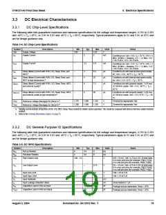
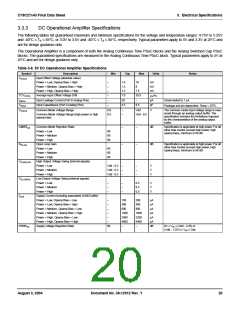
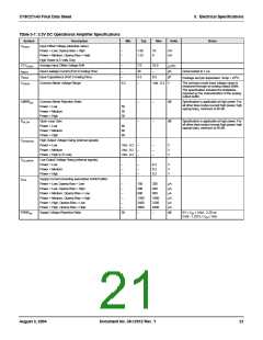
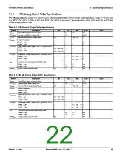
CY8C27x43 Final Data Sheet
3. Electrical Specifications
3.3.5
DC Switch Mode Pump Specifications
The following table lists guaranteed maximum and minimum specifications for the voltage and temperature ranges: 4.75V to 5.25V
and -40°C ≤ TA ≤ 85°C, or 3.0V to 3.6V and -40°C ≤ TA ≤ 85°C, respectively. Typical parameters apply to 5V and 3.3V at 25°C and
are for design guidance only.
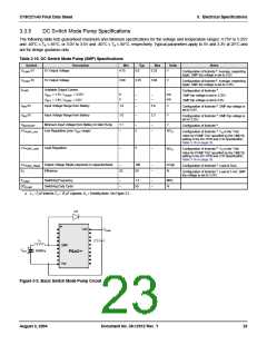
Table 3-10. DC Switch Mode Pump (SMP) Specifications
Symbol
Description
Min
4.75
Typ
5.0
Max
5.25
Units
Notes
Configuration of footnote a. Average, neglecting
ripple. SMP trip voltage is set to 5.0V.
VPUMP 5V
5V Output Voltage
3V Output Voltage
V
V
Configuration of footnote a. Average, neglecting
ripple. SMP trip voltage is set to 3.25V.
VPUMP 3V
IPUMP
3.00
3.25
3.60
Configuration of footnote a
.
Available Output Current
VBAT = 1.5V, VPUMP = 3.25V
8
5
–
–
–
–
mA
mA
SMP trip voltage is set to 3.25V.
SMP trip voltage is set to 5.0V.
VBAT = 1.8V, VPUMP = 5.0V
Configuration of footnote a. SMP trip voltage is
set to 5.0V.
V
BAT5V
BAT3V
Input Voltage Range from Battery
1.8
–
5.0
V
Configuration of footnote a. SMP trip voltage is
set to 3.25V.
V
Input Voltage Range from Battery
1.0
–
3.3
V
Configuration of footnote a
.
VBATSTART
Minimum Input Voltage from Battery to Start Pump
Line Regulation (over VBAT range)
1.1
–
–
5
–
–
V
Configuration of footnote a. VO is the “Vdd
∆VPUMP_Line
%VO
Value for PUMP Trip” specified by the VM[2:0]
setting in the DC POR and LVD Specification,
Table 3-16 on page 26.
Configuration of footnote a. VO is the “Vdd
∆VPUMP_Load
Load Regulation
–
5
–
%VO
Value for PUMP Trip” specified by the VM[2:0]
setting in the DC POR and LVD Specification,
Table 3-16 on page 26.
Configuration of footnote a. Load is 5mA.
∆VPUMP_Ripple Output Voltage Ripple (depends on capacitor/load)
–
100
50
–
–
mVpp
%
Configuration of footnote a. Load is 5 mA. SMP
trip voltage is set to 3.25V.
E3
Efficiency
35
FPUMP
Switching Frequency
Switching Duty Cycle
–
–
1.3
50
–
–
MHz
%
DCPUMP
a. L = 2 µH inductor, C = 10 µF capacitor, D = Schottky diode. See Figure 3-2.
1
1
1
D1
Vdd
VPUMP
L1
C1
SMP
Vss
+
VBAT
TM
Battery
PSoC
Figure 3-2. Basic Switch Mode Pump Circuit
August 3, 2004
Document No. 38-12012 Rev. *I
23

 CYPRESS [ CYPRESS ]