CY8C27x43 Final Data Sheet
3. Electrical Specifications
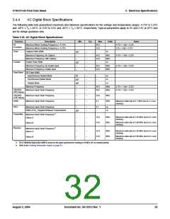
3.4
AC Electrical Characteristics
3.4.1
AC Chip-Level Specifications
The following table lists guaranteed maximum and minimum specifications for the voltage and temperature ranges: 4.75V to 5.25V
and -40°C ≤ TA ≤ 85°C, or 3.0V to 3.6V and -40°C ≤ TA ≤ 85°C, respectively. Typical parameters apply to 5V and 3.3V at 25°C and
are for design guidance only.
Table 3-18. AC Chip-Level Specifications
Symbol
FIMO
Description
Min
23.4
Typ
Max
24.6a
Units
MHz
Notes
Internal Main Oscillator Frequency
24
24
12
48
Trimmed. Utilizing factory trim values.
24.6a,b
12.3b,c
49.2a,b,d
FCPU1
FCPU2
F48M
CPU Frequency (5V Nominal)
CPU Frequency (3.3V Nominal)
Digital PSoC Block Frequency
0.93
0.93
0
MHz
MHz
MHz
Trimmed. Utilizing factory trim values.
Trimmed. Utilizing factory trim values.
Refer to the AC Digital Block Specifications
below.
24.6b, d
64
F24M
F32K1
F32K2
Digital PSoC Block Frequency
Internal Low Speed Oscillator Frequency
External Crystal Oscillator
0
24
32
MHz
kHz
kHz
15
–
32.768
–
Accuracy is capacitor and crystal dependent.
50% duty cycle.
FPLL
PLL Frequency
–
23.986
–
MHz
Multiple (x732) of crystal frequency.
Jitter24M2
TPLLSLEW
24 MHz Period Jitter (PLL)
PLL Lock Time
–
–
–
600
10
ps
0.5
ms
TPLLSLEWS- PLL Lock Time for Low Gain Setting
LOW
0.5
–
50
ms
TOS
External Crystal Oscillator Startup to 1%
–
–
1700
2800
ms
ms
2620
3800
TOSACC
External Crystal Oscillator Startup to 100 ppm
The crystal oscillator frequency is within 100 ppm of its
final value by the end of the Tosacc period. Correct
operation assumes a properly loaded 1 uW maximum
drive level 32.768 kHz crystal. 3.0V ≤ Vdd ≤ 5.5V, -40
oC ≤ TA ≤ 85 oC.
Jitter32k
TXRST
32 kHz Period Jitter
–
100
–
ns
External Reset Pulse Width
10
–
µs
DC24M
24 MHz Duty Cycle
40
–
50
60
–
%
Step24M
Fout48M
24 MHz Trim Step Size
48 MHz Output Frequency
50
kHz
MHz
49.2a,c
46.8
48.0
Trimmed. Utilizing factory trim values.
Jitter24M1
FMAX
24 MHz Period Jitter (IMO)
–
–
600
–
ps
Maximum frequency of signal on row input or row output.
12.3
–
MHz
TRAMP
Supply Ramp Time
0
–
µs
a. 4.75V < Vdd < 5.25V.
b. Accuracy derived from Internal Main Oscillator with appropriate trim for Vdd range.
c. 3.0V < Vdd < 3.6V. See Application Note AN2012 “Adjusting PSoC Microcontroller Trims for Dual Voltage-Range Operation” for information on trimming for operation at 3.3V.
d. See the individual user module data sheets for information on maximum frequencies for user modules.
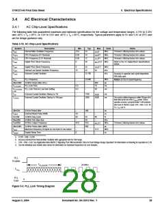
PLL
Enable
T
24 MHz
PLLSLEW
FPLL
PLL
Gain
0
Figure 3-3. PLL Lock Timing Diagram
August 3, 2004
Document No. 38-12012 Rev. *I
28

 CYPRESS [ CYPRESS ]