CY8C27x43 Final Data Sheet
3. Electrical Specifications
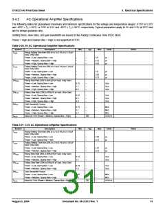
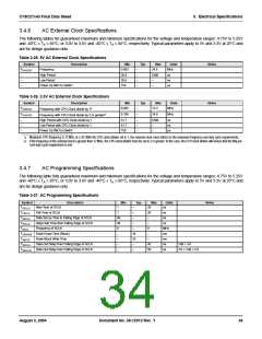
3.4.2
AC General Purpose IO Specifications
The following table lists guaranteed maximum and minimum specifications for the voltage and temperature ranges: 4.75V to 5.25V
and -40°C ≤ TA ≤ 85°C, or 3.0V to 3.6V and -40°C ≤ TA ≤ 85°C, respectively. Typical parameters apply to 5V and 3.3V at 25°C and
are for design guidance only.
Table 3-19. AC GPIO Specifications
Symbol
FGPIO
Description
GPIO Operating Frequency
Min
Typ
Max
Units
MHz
Notes
0
–
12
TRiseF
TFallF
TRiseS
TFallS
Rise Time, Normal Strong Mode, Cload = 50 pF
Fall Time, Normal Strong Mode, Cload = 50 pF
Rise Time, Slow Strong Mode, Cload = 50 pF
Fall Time, Slow Strong Mode, Cload = 50 pF
3
–
18
18
–
ns
ns
ns
ns
Vdd = 4.5 to 5.25V, 10% - 90%
Vdd = 4.5 to 5.25V, 10% - 90%
Vdd = 3 to 5.25V, 10% - 90%
Vdd = 3 to 5.25V, 10% - 90%
2
–
10
10
27
22
–
90%
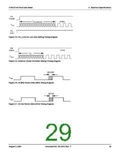
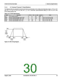
GPIO
Pin
Output
Voltage
10%
TRiseF
TRiseS
TFallF
TFallS
Figure 3-8. GPIO Timing Diagram
August 3, 2004
Document No. 38-12012 Rev. *I
30

 CYPRESS [ CYPRESS ]