CY8C27x43 Final Data Sheet
3. Electrical Specifications
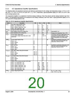
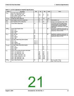
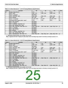
Table 3-7. 3.3V DC Operational Amplifier Specifications
Symbol
VOSOA
Description
Min
Typ
Max
Units
Notes
Input Offset Voltage (absolute value)
Power = Low, Opamp Bias = High
Power = Medium, Opamp Bias = High
High Power is 5 Volts Only
–
–
1.65
10
8
mV
1.32
mV
µV/oC
TCVOSOA
IEBOA
Average Input Offset Voltage Drift
Input Leakage Current (Port 0 Analog Pins)
Input Capacitance (Port 0 Analog Pins)
Common Mode Voltage Range
–
7.0
20
4.5
–
35.0
–
–
pA
Gross tested to 1 µA.
Package and pin dependent. Temp = 25oC.
CINOA
–
9.5
pF
V
VCMOA
0.2
Vdd - 0.2
The common-mode input voltage range is
measured through an analog output buffer.
The specification includes the limitations
imposed by the characteristics of the analog
output buffer.
CMRROA
Common Mode Rejection Ratio
Power = Low
–
–
–
–
dB
dB
Specification is applicable at high power. For
all other bias modes (except high power, high
opamp bias), minimum is 60 dB.
50
50
50
Power = Medium
Power = High
GOLOA
Open Loop Gain
Power = Low
Specification is applicable at high power. For
all other bias modes (except high power, high
opamp bias), minimum is 60 dB.
60
60
80
Power = Medium
Power = High
VOHIGHOA
VOLOWOA
ISOA
High Output Voltage Swing (internal signals)
Power = Low
Vdd - 0.2
Vdd - 0.2
Vdd - 0.2
–
–
–
–
–
–
V
V
V
Power = Medium
Power = High is 5V only
Low Output Voltage Swing (internal signals)
Power = Low
–
–
–
–
–
–
0.2
0.2
0.2
V
V
V
Power = Medium
Power = High
Supply Current (including associated AGND buffer)
Power = Low, Opamp Bias = Low
–
–
–
–
–
–
150
200
µA
µA
µA
µA
µA
µA
Power = Low, Opamp Bias = High
300
400
Power = Medium, Opamp Bias = Low
Power = Medium, Opamp Bias = High
Power = High, Opamp Bias = Low
600
800
1200
2400
4600
1600
3200
6400
Power = High, Opamp Bias = High
PSRROA
Supply Voltage Rejection Ratio
50
–
–
dB
0V ≤ VIN ≤ (Vdd - 2.25) or
(Vdd - 1.25V) ≤ VIN ≤ Vdd.
August 3, 2004
Document No. 38-12012 Rev. *I
21

 CYPRESS [ CYPRESS ]