CY8C27x43 Final Data Sheet
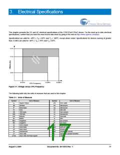
3. Electrical Specifications
3.3
DC Electrical Characteristics
3.3.1
DC Chip-Level Specifications
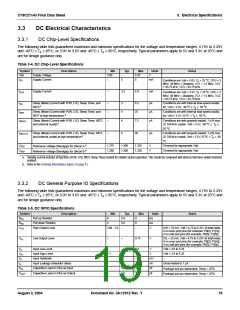
The following table lists guaranteed maximum and minimum specifications for the voltage and temperature ranges: 4.75V to 5.25V
and -40°C ≤ TA ≤ 85°C, or 3.0V to 3.6V and -40°C ≤ TA ≤ 85°C, respectively. Typical parameters apply to 5V and 3.3V at 25°C and
are for design guidance only.
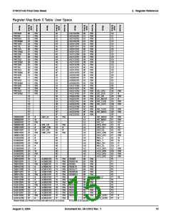
Table 3-4. DC Chip-Level Specifications
Symbol
Vdd
Description
Min
3.00
Typ
Max
5.25
Units
Notes
Supply Voltage
Supply Current
–
5
V
Conditions are Vdd = 5.0V, TA = 25 oC, CPU = 3
IDD
–
8
mA
MHz, 48 MHz = Disabled. VC1 = 1.5 MHz, VC2
= 93.75 kHz, VC3 = 93.75 kHz.
Conditions are Vdd = 3.3V, TA = 25 oC, CPU = 3
IDD3
Supply Current
–
3.3
6.0
mA
MHz, 48 MHz = Disabled, VC1 = 1.5 MHz, VC2
= 93.75 kHz, VC3 = 93.75 kHz.
ISB
Sleep (Mode) Current with POR, LVD, Sleep Timer, and
WDT.a
–
–
–
3
4
4
6.5
25
µA
µA
µA
Conditions are with internal slow speed oscilla-
tor, Vdd = 3.3V, -40 oC ≤ TA ≤ 55 oC.
ISBH
Sleep (Mode) Current with POR, LVD, Sleep Timer, and
WDT at high temperature.a
Conditions are with internal slow speed oscilla-
tor, Vdd = 3.3V, 55 oC < TA ≤ 85 oC.
ISBXTL
Sleep (Mode) Current with POR, LVD, Sleep Timer, WDT,
and external crystal.a
7.5
Conditions are with properly loaded, 1 µW max,
32.768 kHz crystal. Vdd = 3.3V, -40 oC ≤ TA
55 oC.
≤
ISBXTLH
Sleep (Mode) Current with POR, LVD, Sleep Timer, WDT,
and external crystal at high temperature.a
–
5
26
µA
Conditions are with properly loaded, 1 µW max,
32.768 kHz crystal. Vdd = 3.3V, 55 oC < TA ≤ 85
oC.
Reference Voltage (Bandgap) for Silicon A b
Reference Voltage (Bandgap) for Silicon B b
VREF
VREF
1.275
1.280
1.300
1.300
1.325
1.320
V
V
Trimmed for appropriate Vdd.
Trimmed for appropriate Vdd.
a. Standby current includes all functions (POR, LVD, WDT, Sleep Time) needed for reliable system operation. This should be compared with devices that have similar functions
enabled.
b. Refer to the Ordering Information chapter on page 42.
3.3.2
DC General Purpose IO Specifications
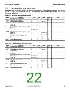
The following table lists guaranteed maximum and minimum specifications for the voltage and temperature ranges: 4.75V to 5.25V
and -40°C ≤ TA ≤ 85°C, or 3.0V to 3.6V and -40°C ≤ TA ≤ 85°C, respectively. Typical parameters apply to 5V and 3.3V at 25°C and
are for design guidance only.
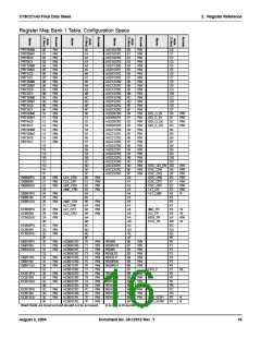
Table 3-5. DC GPIO Specifications
Symbol
Description
Min
Typ
5.6
Max
Units
kΩ
Notes
RPU
Pull up Resistor
4
4
8
8
–
RPD
VOH
Pull down Resistor
High Output Level
5.6
–
kΩ
Vdd - 1.0
V
IOH = 10 mA, Vdd = 4.75 to 5.25V (8 total loads,
4 on even port pins (for example, P0[2], P1[4]),
4 on odd port pins (for example, P0[3], P1[5])).
VOL
Low Output Level
–
–
0.75
0.8
V
IOL = 25 mA, Vdd = 4.75 to 5.25V (8 total loads,
4 on even port pins (for example, P0[2], P1[4]),
4 on odd port pins (for example, P0[3], P1[5])).
VIL
Input Low Level
Input High Level
Input Hysterisis
–
–
V
Vdd = 3.0 to 5.25
Vdd = 3.0 to 5.25
VIH
VH
2.1
–
–
V
60
1
–
mV
nA
pF
pF
IIL
Input Leakage (Absolute Value)
Capacitive Load on Pins as Input
Capacitive Load on Pins as Output
–
–
Gross tested to 1 µA.
Package and pin dependent. Temp = 25oC.
Package and pin dependent. Temp = 25oC.
CIN
COUT
–
3.5
3.5
10
10
–
August 3, 2004
Document No. 38-12012 Rev. *I
19

 CYPRESS [ CYPRESS ]