CY7C9689
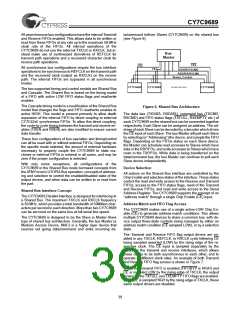
All asynchronous bus configurations have the internal Transmit
and Receive FIFOs enabled. This allows data to be written or
read from these FIFOs at any rate up to the maximum 50-MHz
clock rate of the FIFOs. All internal operations of the
CY7C9689 do not use the external TXCLK or RXCLK, but in-
stead make use of synthesized derivatives of REFCLK for
transmit path operations and a recovered character clock for
receive path operations.
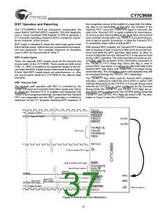
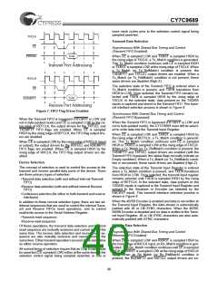
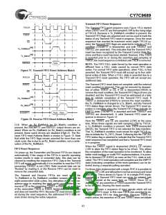
ta/command to/from Slaves (CY7C9689) on the shared bus
(see Figure 6).
Bus
Master
CEn
CE1
All synchronous bus configurations require the bus interface
operations to be synchronous to REFCLK on the transmit path
and the recovered clock (output as RXCLK) on the receive
path. The internal FIFOs are bypassed in all synchronous
modes.
CE2
TXDATA/TXCMD
RXDATA/RXCMD
Status, Control
............
CY7C9689
CY7C9689
CY7C9689
The two supported timing and control models are Shared Bus
and Cascade. The Shared Bus is based on the timing model
of a FIFO with active LOW FIFO status flags and read/write
enables.
The Cascade timing model is a modification of the Shared Bus
model that changes the flags and FIFO read/write enables to
active HIGH. This model is present primarily to allow depth
expansion of the internal FIFO by direct coupling to external
CY7C42x5 synchronous FIFOs. To allow this direct coupling,
the cycle-to-cycle timing between the transmit and receive en-
ables (TXEN and RXEN) are also modified to ensure correct
data transfer.
Figure 6. Shared Bus Architecture
The data bus (TXDATA, RXDATA), command bus (TXCMD,
RXCMD) and FIFO status flags (TXFULL, RXEMPTY, etc.) of
each CY7C9689 on the shared bus can be connected together
respectively. Each Slave can be assigned an address. The ad-
dress of each Slave can be decoded by a decoder which drives
the CE input of each Slave. The bus Master will poll each Slave
by selecting (or “Addressing”) the device, and sample the FIFO
flags. Depending on the FIFOs status on each Slave device,
the Master can schedule read accesses to Slaves which have
data in the RXFIFOs, and write accesses to Slaves which have
room in the TXFIFOs. While data is being transferred on the
data/command bus, the bus Master can continue to poll each
Slave device independently.
These four configurations of bus operation and timing/control
can all be used with or without external FIFOs. Depending on
the specific mode selected, the amount of external hardware
necessary to properly couple the CY7C9689 to state ma-
chines or external FIFOs is minimal in all cases, and may be
zero if the proper configuration is selected.
With only minor exceptions, all configurations of the
CY7C9689 in the Shared Bus mode borrowed concepts from
the ATM Forum’s UTOPIA Bus operation. concepts of address-
ing and selection to control the enabled/disabled state of the
output drivers, and when data can be written to or read from
the part.
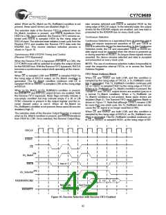
Device Selection
All actions on the Shared Bus interface are controlled by the
Chip Enable and selection states of the interface. These states
control the read and write access to the Receive and Transmit
FIFOs, access to the FIFO status flags, reset of the Transmit
and Receive FIFOs, and read and write access to the Serial
Address Register. The CY7C9689 supports the concept of an
“address match” through a single Chip Enable (CE) input.
Shared Bus Interface Concept
The CY7C9689 Parallel Interface is designed for interfacing to
a Shared Bus. The maximum TXCLK and RXCLK frequency
is 50 MHz, which provides a total bandwidth of 50Million char-
acters per second in each direction. More than two CY7C9689
can be serviced on the same bus at full serial line speed.
Address Match and FIFO Flag Access
The CY7C9689 makes use of a single active-LOW Chip En-
able (CE) to generate address-match conditions. This allows
multiple CY7C9689 devices to share a common bus, with de-
vice output three-state controls being managed by either an
address match condition (CE sampled LOW), or by a selection
state.
The CY7C9689 is designed to be the Slave in Master-Slave
type of shared bus architecture. Generally, the bus Master (a
Medium Access Device, MAC) is a higher layer device that
sources out going data/command and sinks incoming da-
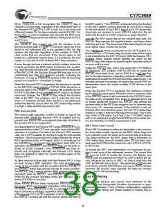
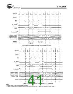
The Transmit and Receive FIFO flag output drivers are en-
abled in any TXCLK, REFCLK, or RXCLK cycle following CE
being sampled asserted (LOW) by the rising edge of the re-
spective clock. The CE input is sampled separately by the
clocks for the transmit and receive interfaces, which allows
these clocks to be both asynchronous to each other, and to
operate at different clock rates. An example of both Transmit
and Receive FIFO flag access is shown in Figure 7.
When the Transmit FIFO is enabled (FIFOBYP is HIGH) and
CE is sampled LOW by the rising edge of TXCLK, the output
drivers for the TXFULL and TXEMPTY FIFO flags are enabled.
When CE is sampled HIGH by the rising edge of TXCLK, these
same output drivers are disabled.
39

 CYPRESS [ CYPRESS ]