CY7C9689
MHz. When configured for synchronous operation (Receive
FIFO is bypassed) data is clocked out of the Receive Output
register at up to 20 MHz when configured for 8-bit characters,
or 16.67 MHz when configured for 10-bit characters. The re-
ceive interface is also configurable for FIFO flags with either
HIGH or LOW status indication
1, and list the functional names of these different signals. Note
that the function of several of these signals changes in different
operating modes. The logical sense of the enable and FIFO
flag signals depends on the intended interface convention and
is set by the EXTFIFO pin.
The transmit interface supports both synchronous and asyn-
chronous clocking modes, each supporting both UTOPIA and
Cascade timing models. The selection of the specific clocking
mode is determined by the RANGESEL and SPDSEL inputs
and the FIFO Bypass (FIFOBYP) signal.
Oscillator Speed Selection
The CY7C9689 is designed to operate over a two-octave
range of serial signaling rates, covering the 50- to 200-MBaud
range. To cover this wide range, the PLLs are configured into
various sub-regions using the SPDSEL and RANGESEL in-
puts, and to a limited extent the BYTE8/10 input. These inputs
are used to configure the various prescalers and clock dividers
used with the transmit and receive PLLs.
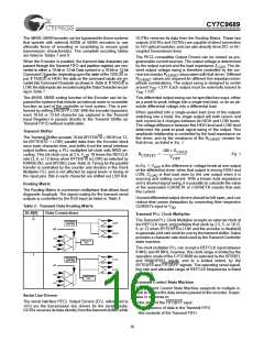
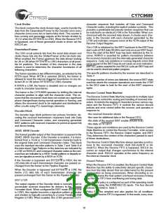
TXDATA[7:0]
TXCMD[3:0]
REFCLK
TXEN
TXCLK
TXSC/D
CE
CY7C9689 TAXI HOTLink Transceiver
Block Diagram Description
12
Transmit Input/Output Register
Transmit Input Register
14
The CY7C9689 provides a synchronous interface for data and
command inputs, instead of the TAXI’s asynchronous strobed
interface. The Transmit Input Register, shown in Figure 2, cap-
tures the data and command to be processed by the HOTLink
Transmitter, and allows the input timing to be made compatible
with asynchronous or synchronous host system buses. These
buses can take the form of external FIFOs, state machines, or
other control structures. Data and command present on the
TXDATA[9:0] and TXSC/D inputs are captured at the rising
edge of the selected sample clock. The transmit data bus bit-
assignments vary depending on the data encoding and bus-
width selected. These bus bit-assignments are shown in Table
Transmit FIFO
To Encoder
Block
Figure 2. Transmit Input Register
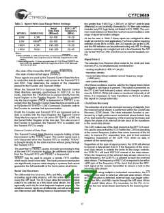
Table 1. Transmit Input Bus Signal Map
[1]
Transmit Encoder Mode
Encoded 8-bit
Pre-encoded 10-bit
Character Stream
Encoded 10-bit
Pre-encoded 12-bit
Character Stream
[2]
[3]
TXDATA Bus Input Bit
TXSC/D
Character Stream
Character Stream
TXSC/D
TXSC/D
[4]
[5]
TXDATA[0]
TXDATA[0]
TXDATA[1]
TXDATA[2]
TXDATA[3]
TXDATA[4]
TXDATA[5]
TXDATA[6]
TXDATA[7]
TXCMD[3]
TXCMD[2]
TXCMD[1]
TXCMD[0]
TXD[0]
TXDATA[0]
TXDATA[1]
TXDATA[2]
TXDATA[3]
TXDATA[4]
TXDATA[5]
TXDATA[6]
TXDATA[7]
TXDATA[8]
TXD[0]
TXDATA[1]
TXD[1]
TXD[2]
TXD[3]
TXD[4]
TXD[5]
TXD[6]
TXD[7]
TXD[8]
TXD[9]
TXD[1]
TXD[2]
TXD[3]
TXD[4]
TXD[5]
TXD[6]
TXD[7]
TXD[8]
TXD[9]
TXDATA[2]
TXDATA[3]
TXDATA[4]
TXDATA[5]
TXDATA[6]
TXDATA[7]
TXDATA[8]/TXCMD[3]
TXDATA[9]/TXCMD[2]
TXCMD[1]
[3]
TXDATA[9]
[5]
TXCMD[1]
TXCMD[0]
TXD[10]
TXCMD[0]
TXD[11]
Notes:
1. All open cells are ignored.
2. When ENCBYP is HIGH and BYTE8/10 is HIGH, transmitted bit order is the encoded form (MSB to LSB) of TXDATA[7,6,5,4] and TXDATA[3,2,1,0] or
TXCMD[3,2,1,0] as selected by TXSC/D.
3. When ENCBYP is HIGH and BYTE8/10 is LOW, transmitted bit order is the encoded form (MSB to LSB) of TXDATA[8,7,6,5,4] and TXDATA[9,3,2,1,0] or
TXCMD[1,0] as selected by TXSC/D.
4. When ENCBYP is LOW and BYTE8/10 is HIGH, the transmitted bit order is (LSB to MSB) TXD[0,1,2,3,4,5,6,7,8,9].
5. When ENCBYP is LOW and BYTE8/10 is LOW, the transmitted bit order is (LSB to MSB) TXD[0,1,2,3,4,5,6,7,8,9,11,10].
14

 CYPRESS [ CYPRESS ]