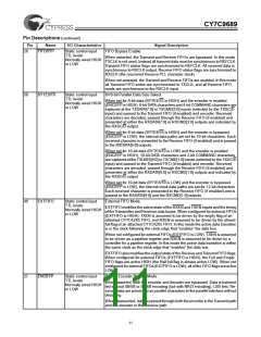
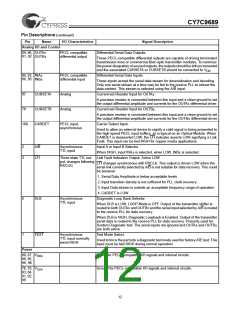
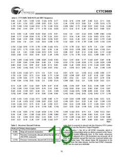
CY7C9689
Synchronous Interface
ed), data is captured in the transmit input register and stored
into the Transmit FIFO. All Transmit FIFO write operations are
clocked by TXCLK.
Synchronous interface clocking operates the entire transmit
data path synchronous to REFCLK. It is enabled by connecting
FIFOBYP LOW to disable the internal FIFOs.
The Transmit FIFO presents Full, Half-Full, and Empty FIFO
flags. These flags are provided synchronous to TXCLK. When
the Transmit FIFO is enabled, it allows operation with a Moore-
type external controlling state machine. When configured for
Cascade timing, the timing and active levels of these signals
are also designed to support direct expansion to Cypress
CY7C42x5 synchronous FIFOs.
Asynchronous Interface
Asynchronous interface clocking controls the writing of host
bus data into the Transmit FIFO. It is enabled by setting
FIFOBYP HIGH to enable the internal FIFOs. In these config-
urations, all writes to the Transmit Input Register, and associ-
ated transfers to the Transmit FIFO, are controlled by TXCLK.
The remainder of the transmit data path is clocked by REFCLK
or synthesized derivatives of REFCLK.
Regardless of bus width (8- or 10-bit characters) the Transmit
FIFO can be clocked at any rate from DC to 50 MHz. This gives
the Transmit FIFO a maximum bandwidth of 50 million charac-
ters per second. Since the serial outputs can only move 20
million characters per second at their fastest operating rate,
there is ample time to service multiple CY7C9689 HOTLinks
with a single controller.
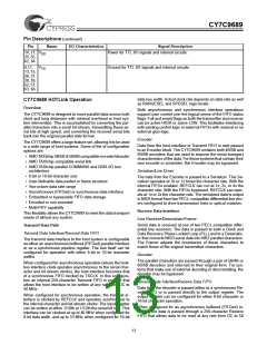
Shared Bus Timing Model
The Shared Bus Timing Model allows multiple CY7C9689
transmitters to be accessed from a common host bus. It is
enabled by setting EXTFIFO LOW. In shared bus timing, the
TXEMPTY and TXFULL outputs and TXEN input are all active
LOW signals. If the CY7C9689 is addressed by asserting CE
LOW, it becomes “selected” when TXEN is asserted LOW. Fol-
lowing selection, data or command is written into the Transmit
FIFO on every clock cycle where TXEN remains LOW.
The read port of the Transmit FIFO is connected to a logic
block that performs data formatting and validation. All data
read operations from the Transmit FIFO are controlled by a
Transmit Control State Machine that operates synchronous to
REFCLK.
Encoder Block
Cascade Timing Model
The Encoder logic block performs two primary functions: en-
coding the data for serial transmission and generating BIST
(Built-In Self-Test) patterns to allow at-speed link and device
testing.
The Cascade timing model is a variation of the shared bus
timing model. Here the TXEMPTY and TXFULL outputs, and
TXEN input, are all active HIGH signals. Cascade timing
makes use of the same selection sequences as shared bus
timing, but write data accesses use a delayed write. This de-
layed write is necessary to allow direct coupling to external
FIFOs, or to state machines that initiate a write operation one
clock cycle before the data is available on the bus.
BIST LFSR
The Encoder logic block operates on data stored in a register.
This register accepts information directly from the Transmit
FIFO, the Transmit Input Register, the 10/8 Byte-Packer, or
from the Transmit Control State Machine when it inserts spe-
cial characters into the data stream.
Cascade timing is enabled by setting EXTFIFO HIGH.
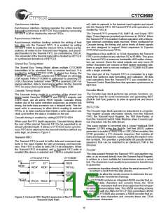
When used for FIFO depth expansion, Cascade timing allows
the size of the internal Transmit FIFO to be expanded to an
almost unlimited depth. It allows a CY7C42x5 series synchro-
nous FIFO to be attached to the transmit interface without any
extra logic, as shown in Figure 3.
This same register is converted into a Linear Feedback Shift
Register (LFSR) when the Built-In Self-Test (BIST) pattern
generator is enabled (TXBISTEN is LOW). When enabled, this
LFSR generates a 511-character sequence that includes all
Data and Special Character codes, including the explicit viola-
tion symbols. This provides a predictable but pseudo-random
sequence that can be matched to an identical LFSR in the
Receiver.
Transmit FIFO
The Transmit FIFO is used to buffer data and command cap-
tured in the input register for later processing and transmis-
sion. This FIFO is sized to hold 256 14-bit characters. When
the Transmit FIFO is enabled, and a Transmit FIFO write is
enabled (the device is selected and TXEN is sampled assert-
Encoder
The data passed through the Transmit FIFO and pipeline reg-
ister, or as received directly from the Transmit Input Register,
is seldom in a form suitable for transmission across a serial
link. The characters must usually be processed or transformed
to guarantee:
CY7C42x5 FIFO
FF* EF*
WEN* REN*
CY7C9689
FF*
TXEN
WEN*
TXFULL
•a minimum transition density (to allow the serial receiver PLL
to extract a clock from the data stream)
•some way to allow the remote receiver to determine the cor-
rect character boundaries (framing).
D
D
Q
TXDATA
TXSC/D
TXCLK
The CY7C9689 contains an integrated 4B/5B encoder that ac-
cepts 8-bit data characters and converts these into 10-bit
transmission characters that have been optimized for transport
on serial communications links. This 4B/5B encoding scheme
is compliant with the ANSI X3T9.5 (FDDI) committee’s 4B/5B
code. The CY7C9689 also contains a 5B/6B encoder that ac-
cepts 10-bit data characters and converts these into 12-bit
transmission characters.
WCLK RCLK
TXCLK
“1”
EXTFIFO
Figure 3. External FIFO Depth Expansion of the CY7C9689
Transmit Data Path
15

 CYPRESS [ CYPRESS ]