CY7C9689
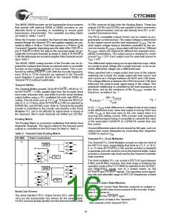
The 4B/5B, 5B/6B encoder can be bypassed for those systems
that operate with external 4B/5B or 5B/6B encoders or use
alternate forms of encoding or scrambling to ensure good
transmission characteristics. The complete encoding tables
are listed in Tables 7 and 8.
OUTB± receives its data from the Routing Matrix. These two
outputs (OUTA± and OUTB±) are capable of direct connection
to +5V optical modules, and can also directly drive DC- or AC-
coupled transmission lines.
The PECL-compatible Output Drivers can be viewed as pro-
grammable current sources. The output voltage is determined
When the Encoder is enabled, the transmit data characters (as
passed through the Transmit FIFO and pipeline register) are con-
verted to either a 10-bit or 12-bit Data symbol or a 10-bit or 12-bit
Command Character, depending upon the state of the TXSC/D in-
put. If TXSC/D is HIGH, the data on the command inputs are en-
coded into Command Character as shown in Table 8. If TXSC/D is
LOW, the data inputs are encoded using the Data Character encod-
ing in Table 7.
by the output current and the load impedance Z
. The de-
LOAD
sired output voltage swing is therefore controlled by the cur-
rent-set resistor R associated with that driver. Different
CURSET
R
values are required for different line impedance/am-
CURSET
plitude combinations. The output swing is designed to center
around V -1.33V. Each output must be externally biased to
DD
-1.33V.
V
DD
The 4B/5B, 5B/6B coding function of the Encoder can be by-
passed for systems that include an external coder or scrambler
function as part of the controller or host system. This is per-
formed by setting ENCBYP LOW. With the encoder bypassed,
each 10-bit or 12-bit character (as captured in the Transmit
Input Register) is passed directly to the Transmit Shifter (or
Transmit FIFO) without modification.
This differential output-swing can be specified two ways: either
as a peak-to-peak voltage into a single-end load, or as an ab-
solute differential voltage into a differential load.
When specified into a single-ended load (one of the outputs
switching into a load), the single output will both source and
sink current as it changes between its HIGH and LOW levels.
The voltage difference between this HIGH level and LOW level
determine the peak-to-peak signal-swing of the output. This
amplitude relationship is controlled by the load impedance on
Transmit Shifter
The Transmit Shifter accepts 10-bit (BYTE8/10 = HIGH) or 12-
bit (BYTE8/10 = LOW) parallel data from the Encoder block
once each character time, and shifts it out the serial interface
output buffers using a PLL-multiplied bit-clock with NRZI en-
coding. This bit-clock runs at 2.5, 5, or 10 times the REFCLK
rate (3, 6, or 12 times when BYTE8/10 is LOW) as selected by
RANGESEL and SPDSEL (see Table 3). Timing for the parallel
transfer is controlled by the counter and dividers in the Clock
Multiplier PLL and is not affected by signal levels or timing at
the input pins. Bits in each character are shifted out LSB first.
the driver, and by the resistance of the R
that driver, as listed in Eq. 1
resistor for
CURSET
180 × Z
LOAD
R
= --------------------------------
Eq. 1
CURSET
V
OPP
In Eq. 1, V
is the difference in voltage levels at one output
OPP
of the differential driver when that output is driving HIGH and
LOW, Z is that load seen by the one output when it is
LOAD
sourcing and sinking current. With a known load impedance
and a desired signal swing, it is possible to calculate the value
of the associated CURSETA or CURSETB resistor that sets
this current.
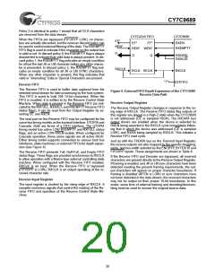
Routing Matrix
The Routing Matrix is a precision multiplexor that allows local
diagnostic loopback. The signal routing for the transmit serial
outputs is controlled by the DLB input as listed in Table 2.
Unused differential output drivers should be left open, and can
reduce their power dissipation by connecting their respective
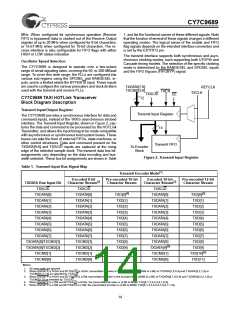
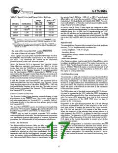
Table 2. Transmit Data Routing Matrix
CURSETx input to V
.
DD
DLB[0]
Data Connections
Transmit PLL Clock Multiplier
0
The Transmit PLL Clock Multiplier accepts an external clock at
the REFCLK input, and multiples that clock by 2.5, 5, or 10 (3,
6, or 12 when BYTE8/10 is LOW and the encoder is disabled)
to generate a bit-rate clock for use by the transmit shifter. It also
provides a character-rate clock used by the Transmit Controller
state machine.
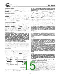
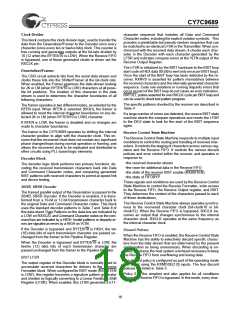
TRANSMIT
SHIFTER
OUTA
OUTB
A/B
INB
RECEIVE
PLL
INA
The clock multiplier PLL can accept a REFCLK input between
8 MHz and 40 MHz, however, this clock range is limited by the
operation mode of the CY7C9689 as selected by the SPDSEL
and RANGESEL inputs, and to a limited extent, by the
BYTE8/10 and FIFOBYP signals. The operating serial signal-
ling rate and allowable range of REFCLK frequencies is listed
in Table 3.
1
TRANSMIT
SHIFTER
OUTA
OUTB
A/B
INB
INA
RECEIVE
PLL
Transmit Control State Machine
The Transmit Control State Machine responds to multiple in-
puts to control the data stream passed to the encoder. It oper-
ates in response to:
Serial Line Drivers
The serial interface PECL Output Drivers (ECL referenced to
+5V) are the transmission line drivers for the serial media.
OUTA± receives its data directly from the transmit shifter, while
•the state of the FIFOBYP input
•the presence of data in the Transmit FIFO
•the contents of the Transmit FIFO
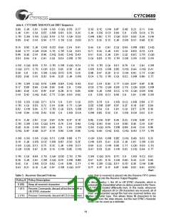
16

 CYPRESS [ CYPRESS ]