CX82100 Home Network Processor Data Sheet
13.3
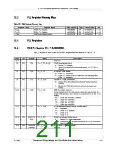
PLL Register Memory Map
Table 13-7. PLL Register Memory Map
Register Label
Register Name
FCLK PLL Register
BCLK PLL Register
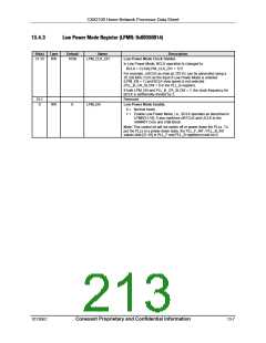
Low Power Mode Register
ASB Address
0x00350068
0x0035006C
0x00350014
Type
RW
RW
Default Value
0x18D04DEA
0x184E2730
0x00000000
Ref.
13.4.1
13.4.2
13.4.3
PLL_F
PLL_B
LPMR
RW
13.4
PLL Registers
13.4.1
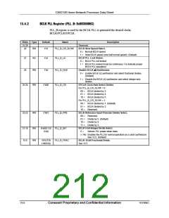
FCLK PLL Register (PLL_F: 0x00350068)
PLL_F register is used by the FCLK PLL to generated the desired FCLK/UCLK.
Bit(s)
31:29
28
Type
Default
Name
Description
Reserved.
FCLK Slow Speed Select.
0 = Normal FCLK speed.
RW
1’b1
PLL_F_CR_SLOW
1 = Slow FCLK speed (one-half normal speed), FCLK = UCLK.
(Default)
FCLK PLL Lock Status.
0 = FCLK PLL not locked.
27
26
RO
RW
1’b1
1’b0
PLL_F_LK
1 = FCLK PLL locked (must be continuous 1 to indicate proper
FCLK PLL operation).
PLL_F_DDS
Disable FCLK ∆Σ Synthesizer.
0 = Enable FCLK ∆Σ synthesizer and select fractional divides.
(Default)
1 = Disable the FCLK ∆Σ synthesizer and select integer-only
divides.
USB Clock Rate Indicate.
25:24
23:22
RW
RW
2’b00
2’b11
PLL_F_CR
These bits indicate to the USB interface block the rate of UCLK. For
proper USB operation, UCLK should be programmed to 48, 60, 72, or
84 MHz.
00 = UCLK rate is 48 MHz. (Default)
01 = UCLK rate is 60 MHz.
10 = UCLK rate is 72 MHz.
11 = UCLK rate is 84 MHz.
FCLK Reference Input Prescale Divider Select.
00 = Reserved.
PLL_F_PRE
01 = Divide by 5. (Default)
10 = Divide by 4.
11 = Divide by 3.
FCLK 6-bit Integer Divide Select.
21:16
15:0
RW
RW
6’b010110
(22d)
PLL_F_INT
0 =
Selects PLL power-down state.
≥ 14d Enables the PLL for normal operation as a clock synthesizer.
See 13.5. (Default)
16’h4DEA
(19946d)
PLL_F_FRAC
FCLK 16-bit Fractional Divide.
See 13.5.
101306C
Conexant Proprietary and Confidential Information
13-5

 CONEXANT [ CONEXANT SYSTEMS, INC ]