CX82100 Home Network Processor Data Sheet
13
Clock Generation Interface Description
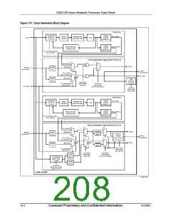
The Clock Generation (CLKGEN) block generates internal and external clocks using two
programmable, fractional multiply phase locked loop (PLL) blocks, FCLK_PLL and
BCLK_PLL (Figure 13-1).
Included in each block is the actual PLL circuit with a voltage-controlled oscillator
(VCO) and post-PLL generation logic which divides the output of each PLL to create a
series of sub-multiple clocks.
Clock generation operation is controlled by the PLL Bypass (PLLBP) input pin and by
three registers: FCLK PLL Register (PLL_F), BCLK PLL Register (PLL_B), and Low
Power Mode Register (LPMR).
PLLBP input low selects PLL Normal Mode (see Section 13.1) and PLLBP input high
selects PLL Bypass Mode for factory clock test operation (see Section 13.7).
The signals on the FCLKIO/GPIO39 and BCLKIO/GPIO38 pins are also controlled by
the PLLBP pin and by the GPIO_Sel7 and GPIO_Sel6 control bits in the GPIO Optional
Register (GPIO_OPT, see Section 9.3.1), respectively. FCLKIO/GPIO39 pin control is
summarized in Table 13-1 and BCLKIO/GPIO38 pin control is summarized in Table
13-2.
When in PLL Bypass Mode, the FCLKIO and BCLKIO pins are configured as inputs,
and are divided and used in place of the PLL outputs. When in PLL Normal Mode, the
FCLKIO and BCLKIO pins can be configured as outputs, and provide a means to
indirectly observe the frequency of the internal clocks generated by the PLLs.
Table 13-1. FCLKIO/GPIO39 Pin Usage Control
PLLBP Input
Pin Voltage
Level
GPIO_Sel7 Bit in
Signal on
Pin Signal
Direction
GPIO Option Register (GPIO_OPT)
FCLKIO/GPIO39 Pin
Low
0
1
1
I/O
O
I
GPIO39
Low
2
UCLK
High
Don’t care
2
XFCLK
Notes:
1. Default at power up reset.
2. See Figure 13-1.
Table 13-2. BCLKIO/GPIO38 Pin Usage Control
PLLBP Input
Pin Voltage
Level
GPIO_Sel6 Bit in
Signal on
Pin Signal
Direction
GPIO Option Register (GPIO_OPT)
BCLKIO/GPIO38 Pin
Low
0
1
1
I/O
O
I
GPIO38
Low
2
EPCLK
2
XBCLK
High
Don’t care
Notes:
1. Default at power up reset.
2. See Figure 13-1.
101306C
Conexant Proprietary and Confidential Information
13-1

 CONEXANT [ CONEXANT SYSTEMS, INC ]