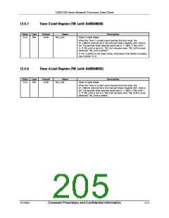
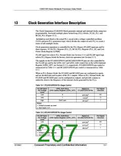
CX82100 Home Network Processor Data Sheet
13.1
PLL Normal Mode
When input pin PLLBP is low, the PLL output clocks are generated based on an
externally provided reference clock frequency on the CLKI pin, typically sourced from
an external oscillator. The CLKI frequency can range from 20 MHz to 40 MHz, 50%
duty cycle.
FCLK_PLL creates a family of frequencies related to 12 MHz. FCLK_PLL is typically
programmed to output 96, 120 144, or 168 MHz. The FCLK output is used directly by
the ARM9TDMI Core when programmed to asynchronous or synchronous modes (see
ARM documents). FCLK is divided by 2 to create UCLK for use by the USB Interface.
UCLK is the clock reference for USB timing, which requires a multiple of 12 MHz, with
a minimum frequency of 48 MHz.
BCLK_PLL creates a family of frequencies related to 25 MHz. BCLK_PLL is typically
programmed to output 50, 75 or 100 MHz. The BCLK output is used directly as the ASB
bus clock. BCLK is divided by 2 to create PCLK for the APB bus, and EPCLK (25 MHz)
for use by a separate Ethernet PHY device.
FCLK_PLL and BCLK_PLL each employ an independently controlled M.N fractional
divider in its PLL feedback circuit in order to synthesize frequencies which are not
integer multiples of the reference clock on CLKI.
The HNP defaults its clocks to “slow mode”, meaning both the BCLK and FCLK are
operating at a slower frequency than is used in typical applications. This facilitates lower
power consumption immediately following power-on-reset. Typical applications will
program the PLLs to output higher frequencies at an appropriate time, e.g., after USB
enumeration.
Pins FCLKIO and BCLKIO can be configured to output clocks FCLK and EPCLK,
respectively, through the GPIO Option register (Section 9.3.1). Both pins default to GPIO
inputs immediately following power-on-reset.
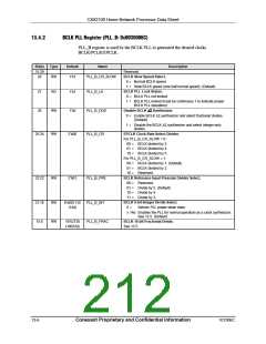
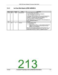
The FCLK_PLL and the BCLK_PLL are implemented using 16-bit delta sigma (ƌ)
synthesizers. FCLK_PLL is programmed by writing to the appropriate bits in the PLL_F
Register (see Section 13.4.1) and BCLK_PLL is programmed by writing to the
appropriate bits in the PLL_B Register (see Section 13.4.2). PLL operation is also
controlled by the Low Power Mode Register (LPMR) (see Section 13.4.3).
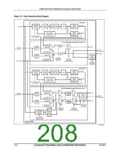
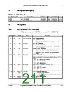
13.2
Generated Clocks
The FCLK PLL and BCLK PLL generated clocks are described in Table 13-3 and Table
13-4, respectively.
FCLK PLL and BCLK PLL generated clock frequencies for various programming
options are listed in Table 13-5 and Table 13-6, respectively.
All clocks are substituted with the JTAG Test Clock (pin TCK) when the HNP is in
boundary scan or internal scan mode.
The ARM940T processor uses BCLK in place of FCLK when in FastBus mode, which is
the default mode immediately following power-on-reset.
101306C
Conexant Proprietary and Confidential Information
13-3

 CONEXANT [ CONEXANT SYSTEMS, INC ]