CX82100 Home Network Processor Data Sheet
13.6
13.7
Watchdog Timer Mode
When Timer 3 is in Watchdog Timer Mode (see Section 12.2), the PLL registers are
disabled from updates by APB writes. This guarantees uninterrupted clocking in the
event a Watchdog Timer timeout and subsequent system reset occurs. There is, however,
a time window when the PLLs can be updated. This occurs when the 7-bit counter that
counts to 100 (incremented every Int_TM3) is equal to 0 or 1. Since this counter is
cleared every time the TM_Lmt3 is written, the time window for allowed PLL updates is
usually open. When the ARM program is not running properly, the window will close,
eventually cause a system reset.
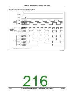
PLL Bypass Mode
If PLLBP is set high, the PLLs are bypassed and the HNP is in test-clock mode with
clocks supplied from the FCLKIO and BCLKIO pins (Figure 13-1). The clock provided
by FCLKIO is called XFCK and the clock provided by BCLKIO is called XBCK. The
clocking requirement is shown in Table 13-9.
Table 13-9. Clocking Requirements
Clock
Maximum
Accuracy
(ppm)
Duty Cycle
(%)
Description
Frequency (MHz)
XFCK
XBCK
144
100
100
100
ARM940T fast clock input
ASB clock
50
50
2
2
In order to setup the test clock mode, configuration control bits must be loaded by pulsing
the CLKI pin. The rising edge of CLKI saves the state of XFCK and XBCK into a control
register (XBCTL, XFCTL) internal to the PLL hardware (and not visible to the software).
The clock used to bypass the VCO in PLL_B is created by the XOR (XBCK, XFCK, and
XBCTL). The clock used to bypass the VCO in PLL_F is created by the XOR (XFCK,
XBCK, and XFCTL). Thus the two PLLs can be bypassed with independent clocks, but
at only ½ the maximum possible frequency, when the control bits are reset to zero. An
internal test VCO bypass clock can be generated at twice the frequency of the external
pin clocks if the XBCK and XFCK are signaled in quadrature (90 degrees out of phase),
and the appropriate control bit(s) is (are) activated (see Figure 13-2).
Note that CLKI also serves as an active-high asynchronous reset for the PLL post-
dividers when PLLBP is high, otherwise the POR is used. The internal bus clocks will
not progress until CLKI is reset low while in test-clock mode.
101306C
Conexant Proprietary and Confidential Information
13-9

 CONEXANT [ CONEXANT SYSTEMS, INC ]