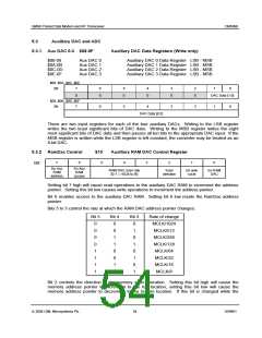
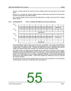
GMSK Packet Data Modem and RF Transceiver
CMX990
Main and Aux PLL
Input
The main and aux PLL circuits have control registers as listed below. Writing to the least significant 8
bits will trigger the circuit to update the dividers with the new multi byte value. Whenever the enable bit
is low the divider circuit will be in the inactive 'zero power' (ZP) mode. To enter normal operation from
ZP mode the MSB (including the enable bit) is written, the LSB would be written last, this would
simultaneously enable the PLL and load the divider ratio - lock may take longer when exiting ZP mode.
To enter ZP mode only the MSB need be written, double buffering will not be used for this control line - a
simple SET / RESET latch will store the 'Enable' value, SET from the output of the 2nd buffer, RESET
from the inverted output of the 1st buffer. The main and aux PLL will control their outputs to the required
quiescent value when shutting down.
Output
One buffered digital output line from each PLL will indicate when the relevant PLL is in lock, this output is
not synchronised. '1' = PLL enabled and in lock, '0' = all other conditions (including disabled ZP state).
These lock outputs are terminated the status register in the host interface block and can optionally cause
an external interrupt to occur. See section 5.2.3 for a description of interrupt operation.
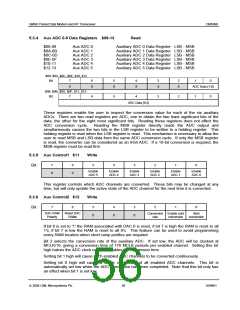
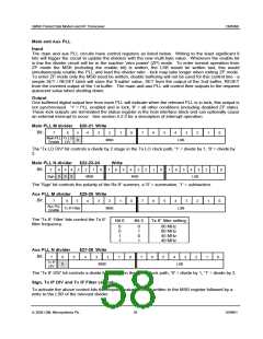
Main PLL M divider
Bit:
$20-21 Write
7
6
5
0
4
3
2
1
0
7
6
5
4
3
2
1
0
Main PLL Tx LO
Enable DIV
MSB
LSB
The 'Tx LO DIV' bit controls a divide by 2 stage in the Tx LO clock path, '1' = divide by 1, '0' = divide by
2.
Main PLL N divider
$22-23-24
Write
Bit:
7
6
0
5
0
4
0
3
2
1
0
7
6
5
4
3
2
1
0
7
6
5
4
3
2
1
0
Sign
MSB
NSB
LSB
The 'Sign' bit controls the polarity of the Rx IF summer, a '0' = summation, '1' = subtraction.
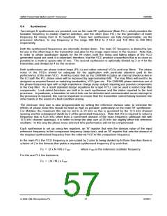
Aux PLL M divider $25-26 Write
Bit:
7
6
5
4
3
2
1
0
7
6
5
4
3
2
1
0
Aux PLL
Enable
Tx IF Filter
MSB
LSB
The 'Tx IF Filter' bits control the Tx IF
filter frequency:
Bit 6
Bit 5
Tx IF filter setting
0
0
1
1
0
1
0
1
90 MHz
80 MHz
45 MHz
40 MHz
Aux PLL N divider
$27-28 Write
Bit:
7
6
0
5
4
3
2
1
0
7
6
5
4
3
2
1
0
Tx IF
DIV
MSB
LSB
The 'Tx IF DIV' bit controls a divide by 2 stage in the Tx IF clock path, '0' = divide by 1, '1' = divide by 2.
Sign, Tx IF DIV and Tx IF Filter control:
To activate the above control bits the required value must be written to the MSB register followed by a
write to the LSB of the relevant divider.
ã 2004 CML Microsystems Plc
58
D/990/1

 CMLMICRO [ CML MICROCIRCUITS ]