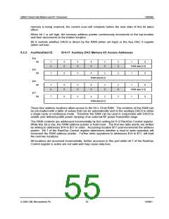
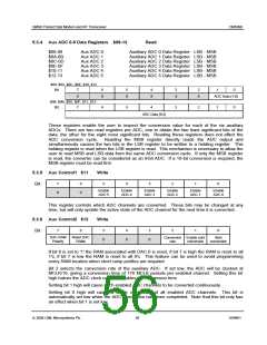
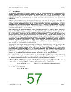
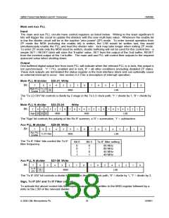
GMSK Packet Data Modem and RF Transceiver
CMX990
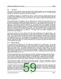
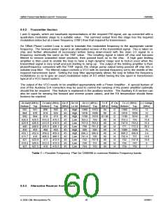
5.5
RF and IF
This comprises the transmitter and receiver parts which, being half duplex, are only operated mutually
exclusively. Normally the non-utilised part will be powered down when not in use. For single antenna
operation an external transmit/receive (T/R) switch is required.
The CMX990 is designed as a broadband RF system. The RF section can support transmission and
reception between 400MHz and 1GHz. As with any RF system care is required with frequency planning
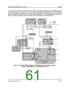
to minimise component count, avoid spurious responses etc. Examples of typical frequency planning are
shown in section 5.5.2.
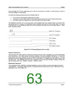
The transmitter takes the baseband I and Q signals from the modem and up-converts them via a
quadrature modulator to a suitable Intermediate Frequency (IF). The summed output from this mixer will
be an FM representation of the required transmit signal but at a lower frequency than that required. An
offset PLL is then used to control an external VCO. The output of the VCO is sampled, usually after
amplification, and mixed down to the IF value; this mixed down signal is then phase/frequency compared
with the IF from the quadrature modulator. The output of the phase comparator is fed to an external loop
filter, which controls the VCO thereby closing the loop. The VCO output then will be an FM signal at the
required RF frequency having a low out-of-band spurious typical of VCO driven transmitters whilst
guaranteeing a modulation index of exactly 0.5. The output of the VCO requires amplifying with an
external PA (Power Amplifier).
The receiver requires use of an external LNA with some pre-filtering and an external balun. The
differential output from the balun goes into an image reject down-mixer to a suitable IF (typically 45
MHz). The IF is filtered with an external filter to remove spurious signals and then goes into an AGC with
a gain control range of 45dB. The output of the AGC is then mixed down to I and Q signals at baseband
via a quadrature mixers. The I and Q signals are then amplified and filtered to remove any signals that
may alias with the subsequent A-D sampling. The amplifier also has a coarse offset removal system to
allow the approximate nulling of DC offsets developed in the circuits that may restrict the dynamic range
in the subsequent processing.
5.5.1 Receiver Section
It is expected that the signal from the T/R switch will be amplified via an external LNA. The use and
positioning of an image reject filtering is up to the radio designer. As a guide, the Mobitex specification
requires a minimum of 45dB of first image rejection of which at least 25dB will be provided by the on-chip
image reject mixer stage. The design is optimised with an LNA gain of about 15dB. It has been
assumed that there is some insertion loss prior to the LNA; but an overall noise figure of 4dB and gain of
10dB (appox.) is achieved by the circuits preceding the CMX990. A digital control is available from the
chip to enable/disable the LNA. A balun must be used to produce a reasonably well-balanced differential
signal to the first mixer on the chip.
The Image Reject Mixer down-converts the signal to 45 MHz, although this frequency may be changed
for use in regions where there may be conflicts with local transmissions. The resulting IF is then output
from the chip as a single ended signal for filtering. It is expected that a relatively low cost crystal filter
can be used to remove spurious signals some distance from the carrier. This is essential to meet the
blocking performance required by the Mobitex specification. For detail filter requirements see Table 2.
The IF-signal from the filter is then taken back on chip to an AGC. This AGC is adjustable in steps of
15dB from -5dB to +40dB. This can be adjusted automatically, if enabled, by the chip or may be
controlled by instruction from the host processor.
The output from the AGC is then mixed down to baseband, by a quadrature mixer stage, to produce I and
Q signals. These are then filtered, to remove unwanted mixer products, spurii and remaining blocking
signals and at the same time amplified to a suitable level for subsequent A-D conversion. The filters also
precondition the signal to prevent aliasing with the A-D sample frequency. Channel filtering is provided
digitally in the baseband processing section.
ã 2004 CML Microsystems Plc
59
D/990/1

 CMLMICRO [ CML MICROCIRCUITS ]