GMSK Packet Data Modem and RF Transceiver
CMX990
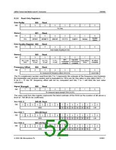
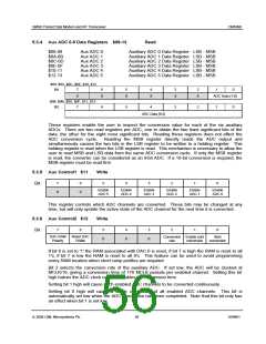
5.3.4 Aux ADC 0-5 Data Registers $08-13
Read
$08-09
$0A-0B
$0C-0D
$0E-0F
$10-11
$12-13
Aux ADC 0
Aux ADC 1
Aux ADC 2
Aux ADC 3
Aux ADC 4
Aux ADC 5
Auxiliary ADC 0 Data Register LSB - MSB
Auxiliary ADC 1 Data Register LSB - MSB
Auxiliary ADC 2 Data Register LSB - MSB
Auxiliary ADC 3 Data Register LSB - MSB
Auxiliary ADC 4 Data Register LSB - MSB
Auxiliary ADC 5 Data Register LSB - MSB
$08, $0A, $0C, $0E, $10, $12
Bit
7
6
5
4
3
2
1
0
X
X
X
X
X
X
ADC Data [1:0]
$09, $0B, $0D, $0F, $11, $13
Bit
7
6
5
4
3
2
1
0
ADC Data [9:2]
These registers enable the user to inspect the conversion value for each of the six auxiliary
ADCs. There are two read registers per ADC, one to obtain the two least significant bits of the
data, the other for the eight most significant bits. Reading these registers does not affect the
ADC conversion cycle. Reading the MSB register directly reads the ADC output and
simultaneously causes the two bits in the LSB register to be written to a holding register. This
holding register is read when the LSB register is read. This mechanism is necessary to allow the
user to read MSB and LSB data from the same ADC conversion cycle. If only the MSB register
is read, the converter can be considered as an 8-bit ADC. If a 10-bit conversion is required, the
MSB register must be read first.
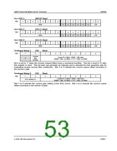
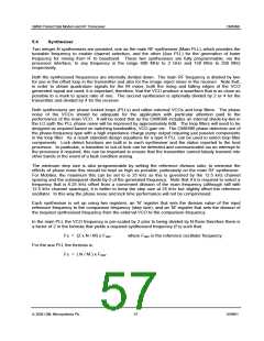
5.3.5 Aux Control1 $11
Write
7
0
6
0
5
4
3
2
1
0
Bit:
Enable
ADC 5
Enable
ADC 4
Enable
ADC 3
Enable
ADC 2
Enable
ADC 1
Enable
ADC 0
This register controls which ADC channels are converted. These bits may be changed at any
time, but will only update the active state of the ADC channel for the next time it is converted.
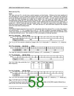
5.3.6 Aux Control2 $12
Write
7
6
5
0
4
0
3
0
2
1
0
Bit:
DAC RAM
Polarity
Reset DAC
RAMs
Conversion Enable cont
rate conversion
Start
conversion
If bit 6 is set to '1' the RAM associated with DAC 0 is reset, if bit 7 is high the RAM is reset to all
1's, if bit 7 is low the RAM is reset to all 0's. This feature can be used to avoid programming
every RAM location when short ramp profiles are required.
Bit 2 selects the conversion rate of the auxiliary ADC. If set low, the ADC will be clocked at
MCLK/16, giving a conversion time of 176 MCLK periods per enabled channel. Setting this bit
high halves the ADC clock rate and doubles the conversion time.
Setting bit 1 high will cause each enabled ADC channels to be converted continuously.
Setting bit 0 high will cause a single conversion of all enabled ADC channels. This bit is
automatically set low when the ADC conversion has been completed. Note that this bit only has
an effect when bit 1 is set low.
ã 2004 CML Microsystems Plc
56
D/990/1

 CMLMICRO [ CML MICROCIRCUITS ]