GMSK Packet Data Modem and RF Transceiver
CMX990
memory is being scanned, the current scan will complete before the new state of this bit takes
effect.
When bit 1 is set high, the memory address pointer continuously increments to the top location
and then decrements to the bottom location.
Bit 0 controls whether DAC0 is driven by the RAM (when set high) or the Aux DAC 0 register
(when set low).
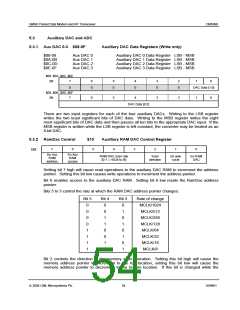
5.3.3 AuxRamData1/2
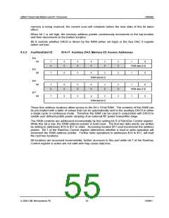
$14-17 Auxiliary DAC Memory I/O Access Addresses
$14
Bit
Bit
7
0
6
0
5
0
4
0
3
0
2
0
1
0
RAM data [1:0]
$15
7
6
5
4
3
2
1
0
RAM data [9:2]
$16
$17
Bit
Bit
7
0
6
0
5
0
4
0
3
0
2
0
1
0
RAM data [1:0]
7
6
5
4
3
2
1
0
RAM data [9:2]
These four address locations allow access to the 64 x 10-bit RAM. The contents of this RAM can
be pre-loaded with a table of values that can be automatically sent to the auxiliary DAC0 in either
a single cycle or continuous mode. Therefore the RAM can be used in conjunction with DAC0 to
enable user defined profile power ramping of an external RF power transmitter stage.
The RAM contents are addressed incrementally by first setting bit 6 of RamDac Control register.
While this bit is low, the RAM address pointer is held reset. The first two data words are written
by writing to addresses $14 to $17 in order. Accessing location $17 post-increments the address
pointer. Bit 7 of the RamDac Control register determines whether a read or write operation will
increment the RAM address pointer. Further write operations to addresses $14 to $17, will load
the next two locations.
All locations are accessed incrementally; further accesses to this port while bit 7 of the RamDac
Control register is active are not valid and may cause data loss.
ã 2004 CML Microsystems Plc
55
D/990/1

 CMLMICRO [ CML MICROCIRCUITS ]