GMSK Packet Data Modem and RF Transceiver
CMX990
6.
Application Notes
6.1
General
The CMX990 chip is a modem and RF system designed for wireless data modem applications. The chip
addresses the needs of various data systems, both product standards and regulatory requirements,
including:
·
·
·
Mobitex Interface Standard (MIS)
European R&TTE ( based on EN 300 113)
FCC Limits (47 CFR Parts 2 and 90)
Details of techniques to meet these requirements can be found in following sections.
6.2 Transmitter
The transmitter architecture is optimised for constant envelope phase/frequency modulation, typically
GMSK or GFSK. The transmitter uses an offset phase locked loop (OPLL) to generate the transmitted
signal. This has the advantage of very low spurious output minimising the need for spurious filtering
reducing the overall cost of the radio and maximising power efficiency due to reduced losses.
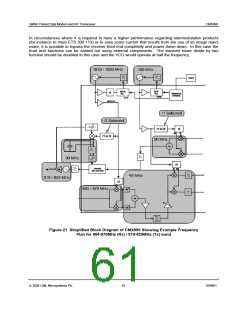
The OPLL works by generating the modulation on an intermediate frequency (IF). This can be set on the
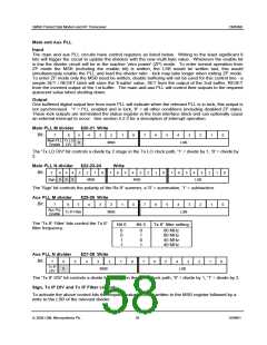
CMX990 by programming the IF PLL to an appropriate IF. Table 1 shows some possible choices for
these values and an example is shown in Figure 21. The CMX990 provides either divide by 2 or divide
by 4 from the programmed local oscillator frequency to aid IF selection. The modulation is generated
using classic I/Q vector modulation to provide an accurate modulated waveform which can also be
inverted to allow high side or low side offset mixing (see section 5.1.4.4). This modulated signal is used
as one input to a phase detector. The output of the phase detector drives a VCO operating directly on
the desired transmitter frequency, via a suitable loop filter. The VCO output can be fed directly to power
amplifier stages. The output of the PA is sampled, a directional coupler is recommended although a
simple sample of the PA output can be used. This is fed to a mixer which translates the output frequency
to the same IF as the reference modulation. The mixer output should be filtered to remove harmonics
which could cause false locking and degrade vector error and is then fed back to the second input of the
phase detector via a limiter. The limiter is used to ensure optimum signal level for the phase detector
and to remove any AM content in the envelope although this should be negligible. The limiter has a wide
input range, this is useful during loop start up as the loop will start locking with very small signals such
that by the time output power rises towards operating levels the loop is already locked and the VCO on
the correct frequency.
Output power can be controlled by the PA gain. This is typically done by applying a suitable ramp to the
PA gate bias. This can be done either open loop or using a power detector and integrator to form a
power levelling feedback loop. Details will depend on the PA device selected to work with the CMX990.
The CMX990 provides a power ramping table on auxiliary DAC 1 to allow a suitable ramp profile to be
applied. The auxiliary ADC can be used for a temperature sensor if software based ramping and output
power compensation is used.
Start up
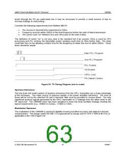
The timing of the turn-on of the transmitter needs careful control. Typical timings are shown in Figure 23.
The first step is to program the IF and RF synthesisers to the correct frequencies for the desired
transmitter channel. When time has been allowed for the PLL’s to lock the transmitter circuits (excluding
the PA) should be enabled. Depending on the leakage through the PA the OPLL should start to lock up.
The limiter has been designed to start to lock with a signal 81dB below the maximum operating power.
For a +35dBm transmitter this is -46dBm or 10dB below the common spurious emissions limit of -36dBm.
The loop should lock quickly and power ramping can start before the loop is fully locked. If leakage
ã 2004 CML Microsystems Plc
62
D/990/1

 CMLMICRO [ CML MICROCIRCUITS ]