GMSK Packet Data Modem and RF Transceiver
CMX990
5.3
Auxiliary DAC and ADC
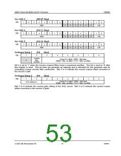
5.3.1 Aux DAC 0-3 $08-0F
Auxiliary DAC Data Registers (Write only)
$08-09
$0A-0B
$0C-0D
$0E-0F
Aux DAC 0
Auxiliary DAC 0 Data Register LSB - MSB
Auxiliary DAC 1 Data Register LSB - MSB
Auxiliary DAC 2 Data Register LSB - MSB
Auxiliary DAC 3 Data Register LSB - MSB
Aux DAC 1
Aux DAC 2
Aux DAC 3
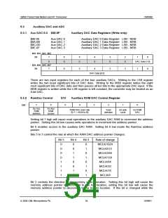
$08, $0A, $0C, $0E
Bit
7
0
6
0
5
0
4
0
3
0
2
0
1
0
DAC Data [1:0]
$09, $0B, $0D, $0F
Bit
7
6
5
4
3
2
1
0
DAC Data [9:2]
There are two input registers for each of the four auxiliary DACs. Writing to the LSB register
writes the two least significant bits of DAC data. Writing to the MSB register writes the eight
most significant bits of DAC data and then passes all ten bits to the appropriate DAC input. If the
MSB register is written while the LSB register is left constant, the converter may be treated as an
8-bit DAC.
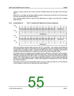
5.3.2 RamDac Control
$10
Auxiliary RAM DAC Control Register
7
6
5
4
3
2
1
0
Bit:
Inc Aux
RAM
address
En Aux
RAM
access
RAM DAC scan rate
[0-7 = /1024 to /8]
Scan
direction
En auto
cycle
En RAM
DAC
Setting bit 7 high will cause read operations to the auxiliary DAC RAM to increment the address
pointer. Setting this bit low causes write operations to increment the address pointer.
Bit 6 enables access to the auxiliary DAC RAM. Setting bit 6 low resets the RamDac address
pointer.
Bits 5 to 3 control the rate at which the RAM DAC address pointer changes:
Bit 5
0
Bit 4
0
Bit 3
0
Rate of change
MCLK/1024
MCLK/512
MCLK/256
MCLK/128
MCLK/64
0
0
1
0
1
0
0
1
1
1
0
0
1
0
1
MCLK/32
1
1
0
MCLK/16
1
1
1
MCLK/8
Bit 2 controls the direction of the memory scan operation. Setting this bit high will cause the
memory address pointer to increment to the top location, setting this bit low will cause the
memory address pointer to decrement to the bottom location. If this bit is changed while the
ã 2004 CML Microsystems Plc
54
D/990/1

 CMLMICRO [ CML MICROCIRCUITS ]