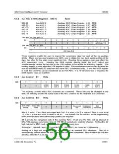
GMSK Packet Data Modem and RF Transceiver
CMX990
5.5.2 Transmitter Section
I and Q signals, which are baseband representations of the required FM signal, are up-converted with a
quadrature modulator stage to a suitable value. The summed output from this stage has the required
modulation index but at a lower frequency (TXIF) than that required for transmission.
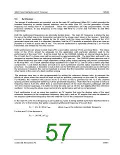
An Offset Phase Locked Loop is used to translate this modulated frequency to the appropriate carrier
frequency. The forward power signal is an attenuated version of the transmitted signal. This is taken on
chip and further attenuated (if necessary) before being down-mixed with the main LO signal to a
frequency nominally the same as the TXIF value. The resulting signal is taken off chip and low-pass
filtered to remove unwanted mixer products, then passed back on to the chip. A high gain limiting
amplifier is then used to enable the loop to have a high dynamic range and to lock-in even when the
transmitted signal is very small and just starting to ramp up. The output of the limiting amplifier is then
phase/frequency compared with the TXIF signal, the charge pump output being passed off chip into a
suitable loop filter. The filtered output controls a VCO with its nominal frequency set to the middle of the
required transmission band. Setting the loop filter appropriately allows the loop to follow the frequency
modulations so as to give an exact modulation index of 0.5 whilst having the low spurii in transmission
typical of a VCO based system.
The output of the VCO needs to be amplified appropriately with a Power Amplifier. A special feature of
one of the Auxiliary D-A converters may be used to control the ramping of the power amplifier optimally
should this be required. This feature is explained in the auxiliary section. The Auxiliary A-D section can
also be used for sensing the forward and reverse power values, and the PA temperature should these
features be required.
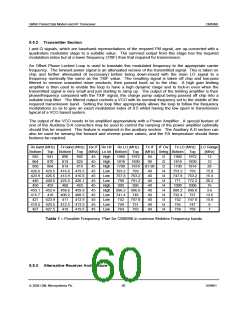
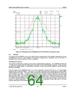
Rx band (MHz) Tx band (MHz) Rx IF Rx Hi/
Rx LO (MHz)
Tx IF IF Div
Tx LO (MHz)
LO Range
(MHz)
Bottom
935
Top
941
Bottom
896
Top
902
825
819
(MHz) Lo bit Bottom
Top
1972
1830
(MHz) Setng Bottom
Top
1972
1830
1818
759
45
45
45
45
45
45
45
45
45
45
45
45
High
High
High
Low
Low
Low
High
High
Low
Low
Low
Low
1960
1818
1790
763.2
84
90
/2
/2
/2
/4
/4
/4
/4
/4
/4
/4
/4
/4
1960
1818
1790
753.2
12
12
864
870
819
850
864
814
1818 81-90
28
426.6
423.9
440
429.5
426.6
440.6
453
416.6 419.5
413.9 416.6
425.5 426.1
769
40
40
40
40
40
40
40
40
40
15.8
15.4
20.2
16
757.8 763.2
747.8 753.2
790
990
791.2
996
771
772.2
1006
450
460
463
1000
453.1
415.7
421
453.4
418
459.6 459.9
406.2 408.5
996.2 996.8
999.2 999.8
3.6
13.6
15.8
6
741.4
752
746
757.8
751
732.4
742
737
747.8
747
423.9
420.5
427.5
411
412.5 413.5
419 419.5
413.9
419.5
427
749
745
764
765
758
759
7
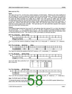
Table 1 – Possible Frequency Plan for CMX990 in common Mobitex Frequency bands
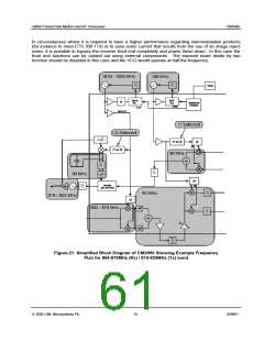
5.5.3 Alternative Receiver Architecture
ã 2004 CML Microsystems Plc
60
D/990/1

 CMLMICRO [ CML MICROCIRCUITS ]