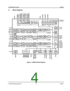
AIS Baseband Processor
CMX910
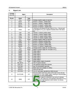
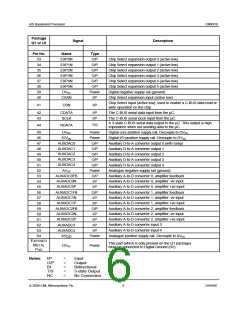
Package
Q1 or L9
Signal
Description
Pin No.
33
Name
Type
O/P
O/P
O/P
O/P
O/P
O/P
Power
I/P
EXP0N
EXP1N
EXP2N
EXP3N
EXP4N
EXP5N
DVSS
Chip Select expansion output 0 (active low)
Chip Select expansion output 1 (active low)
Chip Select expansion output 2 (active low)
Chip Select expansion output 3 (active low)
Chip Select expansion output 4 (active low)
Chip Select expansion output 5 (active low)
Digital negative supply rail (ground)
34
35
36
37
38
39
40
CSXN
Chip Select expansion input (active low)
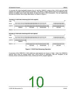
Chip Select input (active low), used to enable a C-BUS data read or
write operation on the chip.
41
CSN
I/P
42
43
CDATA
SCLK
I/P
I/P
The C-BUS serial data input from the µC.
The C-BUS serial clock input from the µC.
A 3-state C-BUS serial data output to the µC. This output is high
impedance when not sending data to the µC.
T/S
44
RDATA
45
46
47
48
49
50
51
52
53
54
55
56
57
58
59
60
61
62
63
64
DVDD
Power
Power
O/P
O/P
O/P
O/P
O/P
Power
O/P
I/P
Digital core positive supply rail. Decouple to DVSS
Digital I/O positive supply rail. Decouple to DVSS
Auxiliary D-to-A converter output 0 (with ramp)
Auxiliary D-to-A converter output 1
IOVDD
AUXDAC0
AUXDAC1
AUXDAC2
AUXDAC3
AUXDAC4
Auxiliary D-to-A converter output 2
Auxiliary D-to-A converter output 3
Auxiliary D-to-A converter output 4
AVSS
Analogue negative supply rail (ground)
Auxiliary A-to-D converter 0, amplifier feedback
Auxiliary A-to-D converter 0, amplifier -ve input
Auxiliary A-to-D converter 0, amplifier +ve input
AUXADC0FB
AUXADC0N
AUXADC0P
I/P
AUXADC1FB
AUXADC1N
AUXADC1P
O/P
I/P
Auxiliary A-to-D converter 1, amplifier feedback
Auxiliary A-to-D converter 1, amplifier -ve input
Auxiliary A-to-D converter 1, amplifier +ve input
I/P
AUXADC2FB
AUXADC2N
AUXADC2P
O/P
I/P
Auxiliary A-to-D converter 2, amplifier feedback
Auxiliary A-to-D converter 2, amplifier -ve input
Auxiliary A-to-D converter 2, amplifier +ve input
Auxiliary A-to-D converter input 3
I/P
AUXADC3
AUXADC4
I/P
Auxiliary A-to-D converter input 4
I/P
AV
DD
Power
Analogue positive supply rail. Decouple to AVSS
EXPOSED
METAL
PAD
This pad (which is only present on the Q1 package)
must be connected to Digital Ground (0V).
DVSS
Power
Notes: I/P
=
=
=
=
=
Input
Output
Bidirectional
3-state Output
No Connection
O/P
BI
T/S
NC
© 2009 CML Microsystems Plc
6
D/910/6

 CMLMICRO [ CML MICROCIRCUITS ]