AIS Baseband Processor
CMX910
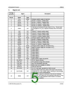
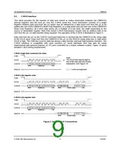
3.
Signal List
Package
Signal
Description
Q1 or L9
Pin No.
Name
AVSS
Type
Power
I/P
1
2
3
4
5
Analogue negative supply rail (ground)
Receive “I” channel 1, positive input
Receive “I” channel 1, negative input
Receive “Q” channel 1, positive input
Receive “Q” channel 1, negative input
IRX1P
IRX1N
QRX1P
QRX1N
I/P
I/P
I/P
A bias line for the internal circuitry, held at ½ AVDD. This pin must
be decoupled to AVSS by a capacitor mounted close to the device
pins
6
VBIAS
O/P
7
ITXP
ITXN
O/P
O/P
O/P
O/P
Power
I/P
Transmit “I” channel, positive output
Transmit “I” channel, negative output
Transmit “Q” channel, positive output
Transmit “Q” channel, negative output
Analogue negative supply rail (ground)
Receive “I” channel 2, positive input
Receive “I” channel 2, negative input
Receive “Q” channel 2, positive input
Receive “Q” channel 2, negative input
Analogue positive supply rail. Decouple to AVSS
Digital I/O positive supply rail. Decouple to DVSS
Enable output 0
8
9
QTXP
QTXN
AVSS
10
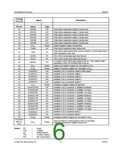
11
12
13
14
15
16
17
18
19
20
21
22
23
24
25
26
27
28
29
30
IRX2P
IRX2N
QRX2P
QRX2N
AVDD
I/P
I/P
I/P
Power
Power
O/P
O/P
O/P
O/P
O/P
O/P
Power
I/P
IOVDD
ENAB0
ENAB1
ENAB2
ENAB3
ENAB4
ENAB5
DVSS
Enable output 1
Enable output 2
Enable output 3
Enable output 4
Enable output 5
Digital negative supply rail (ground)
FSK RF squelch indicator
FSK_MUTE
FSK_DET
FSK_RXD
REFCLK
I/P
FSK baseband energy detect indicator
Raw FSK demodulator input data
Master input clock (multiple of 2.4MHz)
Active low chip reset
I/P
I/P
RESETN
I/P
UTC1PPS
I/P
1Hz UTC sync pulse, typically from GNSS receiver
Slot clock output (active low), pulses at the start of each AIS slot.
Configurable as a ‘wire-ORable’ output, requiring an external pullup
resistor, or as an active pullup/pulldown.
31
SLOTCLKN
IRQN
O/P
O/P
A ‘wire-ORable’ output for connection to the host µC's Interrupt
Request input. This output has a low impedance pull down to DV
when active and is high impedance when inactive. An external
pullup resistor is required.
SS
32
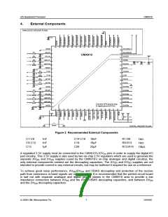
© 2009 CML Microsystems Plc
5
D/910/6

 CMLMICRO [ CML MICROCIRCUITS ]