AIS Baseband Processor
CMX910
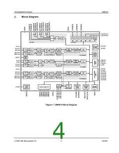
4.
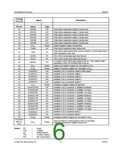
External Components
ANALOGUE GROUND PLANE
AVSS
C18
AVSS
64
63
62
61
60
59
58
57
56
55
54
53
52
51
50
49
AVSS
IRX1P
IRX1N
QRX1P
QRX1N
VBIAS
ITXP
AUXDAC1
AUXDAC0
IOVDD
DVDD
1
48
47
46
45
44
43
42
41
40
39
38
37
36
35
34
33
R1
R2
R3
R4
2
C1
C2
C3
C4
CMX910
IOVDD
AVSS
AVSS
AVSS
3
4
C20
C16
C17
RDATA
SCLK
DVSS
DVSS
DVSS
5
AVSS
R9
6
C13
C9
AVSS
AVSS
AVSS
AVSS
CDATA
CSN
7
R10
R11
R12
ITXN
8
C10
C11
C12
QTXP
QTXN
AVSS
CSXN
9
DVSS
10
11
12
13
14
15
16
DVSS
AVSS
R5
EXP5N
EXP4N
EXP3N
EXP2N
EXP1N
EXP0N
AVSS
IRX2P
IRX2N
QRX2P
QRX2N
AVDD
C5
C6
C7
C8
C19
R6
R7
R8
AVSS
AVSS
AVSS
AVSS
AVSS
Connect QFN ground slug
to digital ground (DVSS
)
C14
AVSS
17
18
19
20
21
22
23
24
25
26
27
28
29
30
31
32
IOVDD
DVDD
DVDD
C15
R13
AVSS
DVSS
Wirelink
AVSS
DVSS
DIGITAL GROUND PLANE
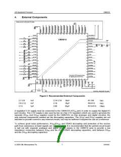
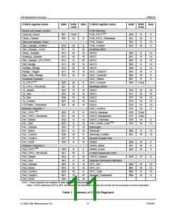
Figure 2 Recommended External Components
C1-C8
1nF
1nF
1µF
C14-C18
C19
10nF
10µF
22µF
R1-R8
1kΩ
C9-C12
C13
R9-R12
R13-R14
1kΩ
C20
10kΩ
A regulated 3.3V supply must be connected to the CMX910’s IOVDD pins in order to supply the digital I/O
pad circuitry. This 3.3V supply is also used by two on-chip 2.5V regulators which are used to generate the
separate AVDD and DVDD supplies (used by the CMX910’s on-chip analogue and digital circuitry), the
only external components needed are the decoupling capacitors. The AVDD and DVDD supplies are not
intended to provide current to any external circuits, but may be buffered if required for use as a reference.
To achieve good noise performance, AVDD/DVDD and VBIAS decoupling and protection of the receive
path from extraneous in-band signals are very important. It is recommended that the printed circuit board
is laid out with separate analogue and digital ground planes in the CMX910 area to provide a low
impedance connection between AVSS and the AVDD/VBIAS decoupling capacitors, and between DVSS
and the DVDD decoupling capacitors.
© 2009 CML Microsystems Plc
7
D/910/6

 CMLMICRO [ CML MICROCIRCUITS ]