AIS Baseband Processor
CMX910
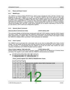
5.
General Description
5.1
Overview of CMX910 Operation
The CMX910 IC has two main receiver circuits that support simultaneous reception of two AIS channels,
or one AIS and one DSC channel. When the two main receive channels are configured for AIS reception,
a supplementary DSC-only receiver can be supported by using a separate external FSK demodulator
(such as the FX604) interfaced to the CMX910. Data bits received on this FSK interface get packed into
bytes and passed through to the host µC. Transmission on a single channel (AIS or DSC) is supported,
during which all reception ceases. The main receive and transmit channels use differential I + Q
signalling, and digital filtering and signal processing techniques are used to obtain a high level of
performance.
The CMX910 also supports the proposed carrier-sensing channel access scheme (CSTDMA) for the AIS
class B standard.
Overall timing synchronisation centres around two counters, one counting the number of samples per slot,
the other the number of slots in a minute. These allow the µC to retrieve slot and sample timing
information for any received message as well as specifying transmit timing accurately. Counters can be
synchronised to an external 1 pulse per second UTC reference signal or allowed to run free, in which
case they must be kept in alignment by the µC.
The CMX910 offers full frame-formatting (HDLC-type) support for AIS receive and transmit, including
NRZI coding, bit stuffing and de-stuffing, training sequence, start/stop flag insertion and deletion, and
CRC generation and checking. A raw mode is also provided allowing greater flexibility. DSC transmission
and reception is only supported in the equivalent of the AIS raw mode.
The transmit channel and three receive channels interface to the µC through individual 32-deep, byte
wide first-in first-out data buffers. These alleviate latency problems and allow higher data rates between
the µC and the CMX910. To allow system performance to be further enhanced, the CMX910 can be
configured to cause an interrupt if the transmit FIFO fill level drops below a user-defined threshold or any
of the receive FIFOs’ fill levels exceed a user-defined threshold.
The CMX910 also assists with power saving and control of critical external RF circuits by providing a
flexible device enable port. Further monitoring and control functions can be implemented using the
integrated auxiliary ADC and DAC circuits.
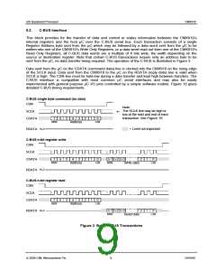
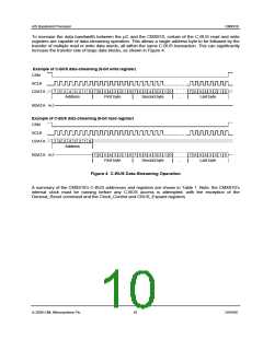
Communication between the CMX910 and the host µC is done through CML’s standard C-BUS interface
and interrupt pin. The C-BUS interface is SPI compatible, and can be driven by an SPI master controller.
A C-BUS expansion port is also provided which allows the connection of up to six further C-BUS or SPI
compatible devices to the µC.
NOTE: To further enhance the CMX910, its Special Command Interface (see section 5.12) can be used
to reconfigure the CMX910’s functionality to fully implement and improve its CS-TDMA reception
capability and slot-clock synchronisation.
© 2009 CML Microsystems Plc
8
D/910/6

 CMLMICRO [ CML MICROCIRCUITS ]