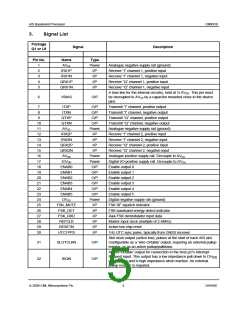
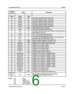
AIS Baseband Processor
CMX910
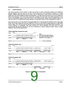
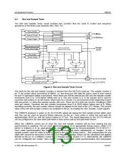
5.2
C-BUS Interface
This block provides for the transfer of data and control or status information between the CMX910’s
internal registers and the host µC over the C-BUS serial bus. Each transaction consists of a single
Register Address byte sent from the µC which may be followed by a data word sent from the µC to be
written into one of the CMX910’s Write Only Registers, or a data word read out from one of the CMX910’s
Read Only Registers; all C-BUS data words are a multiple of 8 bits wide, the width depending on the
source or destination register. Note that certain C-BUS transactions require only an address byte to be
sent from the µC, no data transfer being required. The operation of the C-BUS is illustrated in Figure 3.
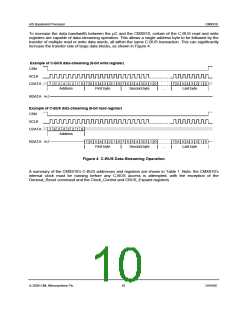
Data sent from the µC on the CDATA (command data) line is clocked into the CMX910 on the rising edge
of the SCLK input. Data sent from the CMX910 to the µC on the RDATA (reply data) line is valid when
SCLK is high. The CSN line must be held low during a data transfer and kept high between transfers. The
C-BUS interface is compatible with most common µC serial interfaces and may also be easily
implemented with general purpose µC I/O pins controlled by a simple software routine. Figure 16 gives
detailed C-BUS timing requirements.
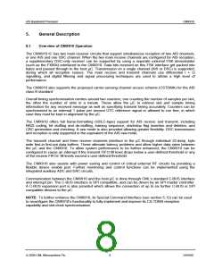
C-BUS single byte command (no data)
CSN
Note:
The SCLK line may be high or
low at the start and end of each
transaction. See Figure 16.
SCLK
←
CDATA
7
MSB
6
5
4
3
2
2
2
1
1
1
0
LSB
Address
Hi-Z
RDATA
= Level not important
C-BUS n-bit register write
CSN
SCLK
CDATA
RDATA
7
MSB
6
5
4
3
0
LSB
n-1 n-2 n-3
2
1
0
LSB
MSB
Address
Write data
Hi-Z
C-BUS n-bit register read
CSN
SCLK
CDATA
RDATA
7
MSB
6
5
4
3
0
LSB
Address
Hi-Z
n-1 n-2 n-3
2
1
0
MSB
LSB
Read data
Figure 3 Basic C-BUS Transactions
© 2009 CML Microsystems Plc
9
D/910/6

 CMLMICRO [ CML MICROCIRCUITS ]