AIS Baseband Processor
CMX910
Table
Page
Table 1 Summary of C-BUS Registers ............................................................................11
Table 2 Example Tx Event Sequence Setup ...................................................................31
Figure
Page
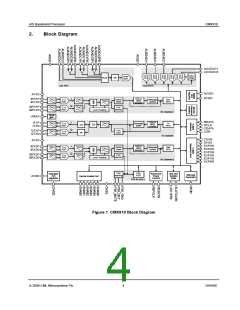
Figure 1 CMX910 Block Diagram ......................................................................................4
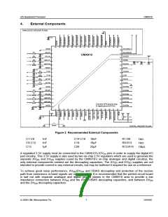
Figure 2 Recommended External Components.................................................................7
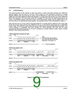
Figure 3 Basic C-BUS Transactions ..................................................................................9
Figure 4 C-BUS Data-Streaming Operation ....................................................................10
Figure 5 Slot and Sample Timer Circuit...........................................................................13
Figure 6 Transmit Channel ..............................................................................................19
Figure 7 Tx (AIS raw mode) state transitions ..................................................................25
Figure 8 Tx (AIS burst mode) state transitions ................................................................27
Figure 9 Tx (DSC mode) state transitions........................................................................28
Figure 10 Typical AIS Transmission ................................................................................29
Figure 11 Receive Channel .............................................................................................32
Figure 12 Auxiliary ADC...................................................................................................40
Figure 13 Auxiliary DACs.................................................................................................42
Figure 14 RAMDAC Values .............................................................................................45
Figure 15 I/Q Filter response in 25kHz operation............................................................59
Figure 16 C-BUS Timing..................................................................................................59
Figure 17 Q1 Mechanical Outline: Order as part no. CMX910Q1..................................60
Figure 18 L9 Mechanical Outline: Order as part no. CMX910L9....................................61
History
Version Changes
Date
1 - 5
Earlier versions, for which a history file is not maintained.
20/11/0
8
6
26/03/0
9
• Corrected description of the operation of the Auto Nudge Acquire sequence in
section 5.4.2.
It is always recommended that you check for the latest product datasheet version from the
Datasheets page of the CML website: [www.cmlmicro.com].
© 2009 CML Microsystems Plc
3
D/910/6

 CMLMICRO [ CML MICROCIRCUITS ]