AIS Baseband Processor
CMX910
CONTENTS
Section
Page
1.
2.
3.
4.
5.
Brief Description .................................................................................................1
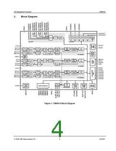
Block Diagram.....................................................................................................4
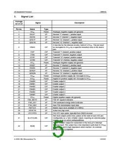
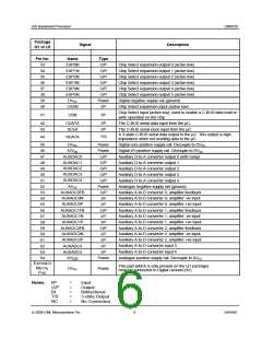
Signal List ............................................................................................................5
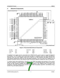
External Components.........................................................................................7
General Description............................................................................................8
5.1
5.2
5.3
Overview of CMX910 Operation............................................................8
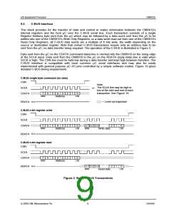
C-BUS Interface......................................................................................9
Reset and Power Control ....................................................................12
5.3.1 RESETN pin .............................................................................12
5.3.2 General Reset Command .......................................................12
5.3.3 Clock Control...........................................................................12
Slot and Sample Timer ........................................................................13
5.4.1 Manual Nudge..........................................................................16
5.4.2 Auto Nudge..............................................................................17
5.4.3 Sleep Mode ..............................................................................17
5.4.4 Selecting the Nudge_Trigger Value ......................................18
Transmit Operation..............................................................................19
5.5.1 Transmitter Registers.............................................................19
5.5.2 AIS Raw Mode Transmit.........................................................24
5.5.3 AIS Burst Mode Transmit.......................................................25
5.5.4 DSC Transmit ..........................................................................27
5.5.5 Transmitter Timing Control....................................................29
Receive Operation................................................................................32
5.6.1 Receiver Registers..................................................................33
5.6.2 AIS Raw Mode Receive...........................................................37
5.6.3 AIS Burst Mode Receive.........................................................38
5.6.4 DSC Receive (Main Channel).................................................39
5.6.5 DSC Receive (External FSK Interface)..................................39
Auxiliary A-to-D Converter..................................................................40
Auxiliary D-to-A Converters................................................................42
Interrupt Generator..............................................................................46
Device Enable Port...............................................................................48
C-BUS Expansion Port ........................................................................49
Special Command Interface................................................................50
5.4
5.5
5.6
5.7
5.8
5.9
5.10
5.11
5.12
6.
7.
Supplementary Information .............................................................................52
6.1 Glossary of Terms................................................................................52
Performance Specification...............................................................................54
7.1
Electrical Performance........................................................................54
7.1.1 Absolute Maximum Ratings...................................................54
7.1.2 Operating Limits......................................................................54
7.1.3 Operating Characteristics......................................................55
Packaging .............................................................................................60
7.2
© 2009 CML Microsystems Plc
2
D/910/6

 CMLMICRO [ CML MICROCIRCUITS ]