TDMA Digital Radio Processor
CMX7161
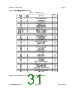
7.12 C-BUS Register Summary
Table 3 C-BUS Registers
Word
Size
(bits)
0
ADDR.
(hex)
READ/
WRITE
REGISTER
$01
W
C-BUS General Reset
$48
$49
$4B
W
W
R
Transmit FIFO
FI Load FIFO
Transmit FIFO Level
Receive FIFO
8
16
8
$4C
R
8
$4D
$4F
$50
R
R
Device Information
Receive FIFO Level
FIFO Control
AuxADC1-4 Control
AuxADC1-4 Threshold
AuxDAC1-4 Control
AuxADC1-4 Read
16
8
W
W
W
W
R
16
16
16
16
16
$51 to $54
$55 to $58
$59 to $5C
$71 to $74
$5D
$5E
$5F
$60
$75
$76
$7A
$7B
W
W
W
W
R
R
R
R
Mod 2 Output Control
Mod 1 Output Control
I Input Control
16
16
16
16
16
16
16
16
Q Input Control
I Input Control Readback
Q Input Control Readback
Receive Status
Frequency Error
$62
$63
$64
$77
$78
$79
W
W
W
R
R
R
SPI Thru-Port Control
SPI Thru-Port Write
GPIO Control
RSSI Value
SPI Thru-Port Read
GPIO Input
16
16
16
16
16
16
$68
$69
$6A
$6B
$6C
$7E
$7F
W
W
W
W
W
R
Slot Control
Modem Options
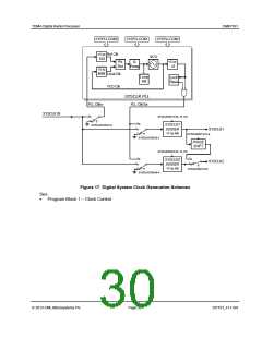
Programming
Modem Control
IRQ Mask
16
16
16
16
16
16
16
IRQ Status
Modem Control Readback
R
$B0
$B1
$B2
$B3
$B4
$B5
$B7
W
W
W
W
W
W
W
I/Q Input Power Control
I Input Coarse Gain
Q Input Coarse Gain
16
16
16
16
16
16
16
Mod 1/2 Output Power Control
Mod 1 Output Coarse Gain
Mod 2 Output Coarse Gain
VBIAS Control
All other C-BUS addresses are reserved and must not be accessed.
2013 CML Microsystems Plc
Page 31
D/7161_FI-1.0/4

 CMLMICRO [ CML MICROCIRCUITS ]