TDMA Digital Radio Processor
CMX7161
8.1.3 Operating Characteristics
Details in this section represent design target values and are not currently guaranteed.
For the following conditions unless otherwise specified:
External components as recommended in Section 5, External Components.
Maximum load on digital outputs = 30pF
TAMB = 40°C to +85°C
AV = DV = 3.0V to 3.6V
DD
DD
Current consumption figures quoted in this section apply to the device when loaded with FI-1 only.
Current consumption may vary with other valid Function Images™.
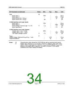
DC Parameters
Notes
Min.
Typ.
1.0
Max.
Unit
µA
11
Supply Current (see also section 8.1.4)
All Powersaved
AI + DI
10,15
15
–
–
–
–
DD
DD
Additional current for one auxiliary
System Clock (output running at 5MHz –
SYSCLKPLL active)
DI (DV = 3.3V, DV = 1.8V)
900
µA
DD
DD
CORE
15
Additional current for one auxiliary
System clock (output running at 4.8MHz –
SYSCLKPLL not required)
DI (DV = 3.3V, DV = 1.8V)
–
–
–
675
190
–
–
–
µA
µA
µA
DD
DD
CORE
15
Additional current for each auxiliary ADC
DI (DV = 3.3V, DV = 1.8V)
DD
DD
CORE
14,15
Additional current for each auxiliary DAC
AI (AV = 3.3V)
210 to 370
DD
DD
Notes:
11 TAMB = 25°C, not including any current drawn from the device pins by external circuitry.
12 System Clocks, Auxiliary circuits disabled, but all other digital circuits (including the Main
Clock PLL) enabled and V
enabled.
BIAS
13 Using a 19.2MHz external clock input.
14 A lower current is measured when outputting the smallest possible dc level from an
AuxDAC, a higher current is measured when outputting the largest possible dc value.
15 Using a 19.2MHz external clock input.
2013 CML Microsystems Plc
Page 33
D/7161_FI-1.0/4

 CMLMICRO [ CML MICROCIRCUITS ]