TDMA Digital Radio Processor
CMX7161
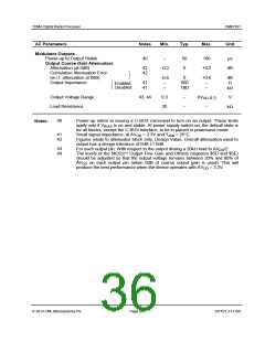
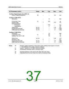
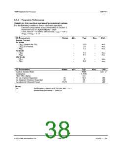
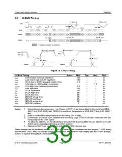
AC Parameters
Notes
Min.
Typ.
Max.
Unit
CLK Input
'High' Pulse Width
'Low' Pulse Width
30
30
15
15
–
–
–
–
ns
ns
Input Impedance (at 9.6MHz)
Powered-up
Resistance
Capacitance
Resistance
Capacitance
–
–
–
–
150
20
300
–
–
–
–
k
pF
k
pF
Powered-down
20
SYSCLK1/2 Outputs
SYSPLL Operating Frequency
SYSCLK1/2 Output Frequency
Rise Time
38
–
–
–
–
–
–
250
20
13.5
6
MHz
MHz
ns
Fall Time
–
ns
V
BIAS
Start-up Time (from powersave)
–
30
–
ms
Differential I and Q Inputs
Input Impedance, Enabled
Input Impedance, Muted or Powersaved
Maximum Input Voltage Excursion
31
32
10
–
200
–
140
k
k
–
20 to 80
%AV
DD
Programmable Input Gain Stage
Gain (at 0dB)
Cumulative Gain Error
33
33
0
0
+0.5
+1.0
dB
dB
0.5
1.0
(w.r.t. attenuation at 0dB)
30
31
32
Timing for an external input to the SYSCLKIN pin.
With no external components connected.
Notes:
For each input pin and for AV = 3.3V, the maximum allowed signal swing is:
DD
(3.3 x 0.8) - (3.3 x 0.2) = 2.0V.
33
Design Value. Overall attenuation input to output has a design tolerance of 0dB
±1.0dB.
2013 CML Microsystems Plc
Page 35
D/7161_FI-1.0/4

 CMLMICRO [ CML MICROCIRCUITS ]