TDMA Digital Radio Processor
CMX7161
7.10.3 Auxiliary DAC/RAMDAC Operation
The four auxiliary DACs are programmed via the AuxDAC1-4 Control - $59 to $5C, write registers.
AuxDAC1 may also be programmed to operate as a RAMDAC which will autonomously output a pre-
programmed profile at a programmed rate. The AuxDAC1-4 Control - $59 to $5C, write register, with b14
set, controls the RAMDAC mode of operation when configured as a manually triggered RAMDAC.
The default profile is a Raised Cosine (see Table 5 in the user manual), but this may be over-written with a
user defined profile by writing to Program Block 0. The AuxDAC outputs hold the user-programmed level
during a powersave operation if left enabled, otherwise they will return to zero.
See:
AuxDAC1-4 Control - $59 to $5C, write
Program Block 0 - RAMDAC
Program Block 1 – Clock Control
7.10.4 SPI Thru-Port
The CMX7161 offers an SPI Thru-Port which allows the host, using the main C-BUS interface, to
command the CMX7161 to read or write up to three external SPI/C-BUS devices attached to the
CMX7161. The CMX7161 acts as an SPI/C-BUS master in this mode, controlling three chip selects, clock
and data out (MOSI), and receiving data in (MISO).
The port can be independently configured for each chip select with clock speed, inter-frame guard period
and clock phase/polarity to match the specification of the slave SPI/C-BUS device attached. The port can
be used for C-BUS operation or in raw SPI mode. In C-BUS mode the data read/written is assumed to be
in the format:
Address byte, data byte 1 (optional), data byte 2 (optional)
The CMX7161, as the master, drives both the address and data for write operations. For read operations it
drives the address and receives the data. Transactions may carry 0, 1 or 2 bytes of data (a zero-byte write
typically being a reset command).
SPI mode is more flexible. No assumption is made about the SPI word format, nor any assumption that
the length is a whole number of bytes.
See:
SPI Thru-Port Control - $62, write
SPI Thru-Port Write - $63, write
SPI Thru-Port Read - $78, read
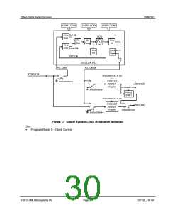
7.11 Digital System Clock Generators
Two System Clock outputs, SYSCLK1 and SYSCLK2, are available to drive additional circuits as required.
The System Clock circuitry is shown in Figure 17 Digital System Clock Generation Schemes.
Having chosen the input frequency source, system clock generation may be done by simply dividing the
input frequency source, or via its own phase locked loop. The system clock PLL does not affect any other
internal operation of the CMX7161 – so if a frequency that is not a simple fraction of the external oscillator
frequency is required, it can be used with no side effects. There is one phase locked loop, with
independent output dividers to provide phase locked output signals.
2013 CML Microsystems Plc
Page 29
D/7161_FI-1.0/4

 CMLMICRO [ CML MICROCIRCUITS ]