CS5525 CS5526
CC, and PS/R bits must be logic 0 and the CB (MSB)
bit must be a logic 1. The register to be written is se-
lected with the RSB2-RSB0 bits of the command
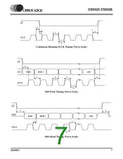
word. Figure 6 illustrates the serial sequence neces-
sary to write to, or read from the serial port.
Reading/Writing On-Chip Registers
The CS5525/26’s offset, gain, and configuration
registers are read/writable while the conversion
data register is read only.
To perform a read from a specific register, the R/W
bit of the command word must be a logic 1. The SC,
CC, and PS/R bits must be logic 0 and the CB
(MSB) bit must be a logic 1. The register to be writ-
ten is selected with the RSB2-RSB0 bits of the
command word.
If the Set-up Registers are chosen with the RSB2-
RSB0 bits, the registers are read or written in the
following sequence: Offset, Gain and Configura-
tion. This is accomplished by following one 8-bit
command word with three 24-bit data words for a
total of 72 data bits.
To perform a write to a specific register, the R/W
bit of the command word must be a logic 0. The SC,
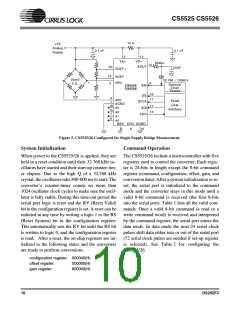
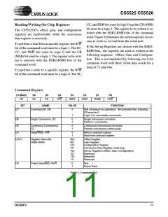
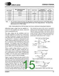
Command Register
D7(MSB)
D6
D5
D4
D3
D2
D1
D0
CB
SC
CC
R/W
RSB2
RSB1
RSB0
PS/R
BIT
NAME
VALUE
FUNCTION
D7
Command Bit, CB
0
Null command (no operation). All command bits, including
CB must be 0.
1
Logic 1 for executable commands.
D6
Single Conversion, SC
0
1
Single Conversion not active.
Perform a conversion.
D5
Continuous Conversions,
CC
0
1
Continuous Conversions not active.
Perform conversions continuously.
D4
Read/Write, R/W
0
1
Write to selected register.
Read from selected register.
D3-D1
Register Select Bit,
RSB2-RSB0
000
001
010
011
100
101
110
111
Offset Register
Gain Register
Configuration Register
Conversion Data Register (read only)
Set-up Registers (Offset, Gain, Configuration)
Reserved
Reserved
Reserved
D0
Power Save/Run, PS/R
0
1
Run
Power Save
Table 1. Command Set
DS202F3
11

 CIRRUS [ CIRRUS LOGIC ]