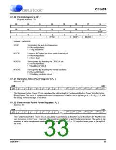
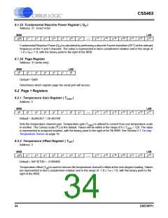
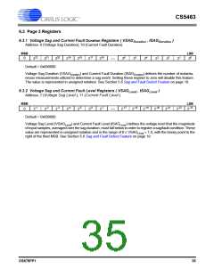
CS5463
7. SYSTEM CALIBRATION
N + 30 conversion cycles to complete. For AC offset cal-
ibrations, the sequence takes at least 6N + 30 ADC cy-
cles to complete, (about 6 computation cycles). As N is
increased, the accuracy of calibration results will in-
crease.
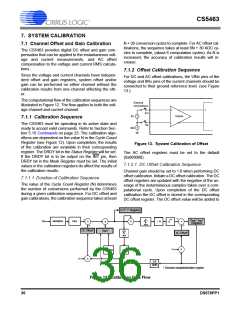
7.1 Channel Offset and Gain Calibration
The CS5463 provides digital DC offset and gain com-
pensation that can be applied to the instantaneous volt-
age and current measurements, and AC offset
compensation to the voltage and current RMS calcula-
tions.
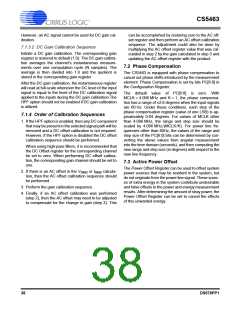
7.1.2 Offset Calibration Sequence
Since the voltage and current channels have indepen-
dent offset and gain registers, system offset and/or
gain can be performed on either channel without the
calibration results from one channel affecting the oth-
er.
For DC and AC offset calibrations, the VIN pins of the
voltage and IIN pins of the current channels should be
connected to their ground reference level. (see Figure
13.)
The computational flow of the calibration sequences are
illustrated in Figure 12. The flow applies to both the volt-
age channel and current channel.
External
Connections
+
-
+
-
AIN+
AIN-
+
-
0V
XGAIN
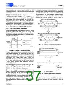
7.1.1 Calibration Sequence
The CS5463 must be operating in its active state and
ready to accept valid commands. Refer to Section Sec-
tion 5.15 Commands on page 23. The calibration algo-
rithms are dependent on the value N in the Cycle Count
Register (see Figure 12). Upon completion, the results
of the calibration are available in their corresponding
register. The DRDY bit in the Status Register will be set.
If the DRDY bit is to be output on the INT pin, then
DRDY bit in the Mask Register must be set. The initial
values in the calibration registers do affect the results of
the calibration results.
+
-
CM
Figure 13. System Calibration of Offset
The AC offset registers must be set to the default
(0x000000).
7.1.2.1 DC Offset Calibration Sequence
Channel gain should be set to 1.0 when performing DC
offset calibration. Initiate a DC offset calibration. The DC
offset registers are updated with the negative of the av-
erage of the instantaneous samples taken over a com-
putational cycle. Upon completion of the DC offset
calibration the DC offset is stored in the corresponding
DC offset register. The DC offset value will be added to
7.1.1.1 Duration of Calibration Sequence
The value of the Cycle Count Register (N) determines
the number of conversions performed by the CS5463
during a given calibration sequence. For DC offset and
gain calibrations, the calibration sequence takes at least
to V*, I* Registers
+
N
+
VRMS*, IRMS
Registers
*
Filter
Modulator
In
X
+
+
N
÷
+
X
√
Σ
+
N
DC Offset*
Gain*
AC Offset*
Σ
X
-1
N
÷
Inverse
X
-1
0.6
RMS
* Denotes readable/writable register
Figure 12. Calibration Data Flow
36
DS678PP1

 CIRRUS [ CIRRUS LOGIC ]