CS5463
each instantaneous measurement to nullify the DC
component present in the system during conversion
commands.
A typical rms calibration value which allows for reason-
able over-range margin would be 0.6 or 60% of the volt-
age and current channel’s maximum input voltage level.
Two examples of AC gain calibration and the updated
digital output codes of the channel’s instantaneous data
registers are shown in Figures 15 and 16. Figure 16
7.1.2.2 AC Offset Calibration Sequence
Corresponding offset registers I
and/or V
ACoff
ACoff
should be cleared prior to initiating AC offset calibra-
tions. Initiate an AC offset calibration.The AC offset reg-
isters are updated with an offset value that reflects the
RMS output level. Upon completion of the AC offset cal-
ibration the AC offset is stored in the corresponding AC
offset register. The AC offset register value is subtract-
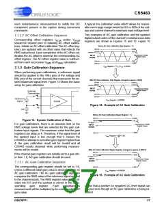
Before AC Gain Calibration (Vgn Register = 1)
250 mV
230 mV
0.9999...
0.92
Sinewave
Instantaneous Voltage
Register Values
INPUT
SIGNAL
0 V
-0.92
-1.0000...
-230 mV
-250 mV
ed from each successive V
and I
calculation.
RMS
RMS
VRMS Register = 230 √2 x1/250 ≈ 0.65054
/
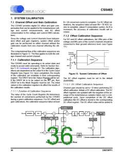
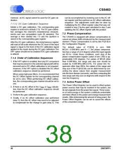
7.1.3 Gain Calibration Sequence
When performing gain calibrations, a reference signal
should be applied to the VIN pins of the voltage and
IIN pins of the current channels that represents the de-
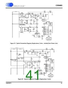
sired maximum signal level. Figure 14 shows the basic
setup for gain calibration.
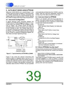
After AC Gain Calibration (Vgn Register changed to approx. 0.9223)
250 mV
230 mV
0.92231
0.84853
Sinewave
INPUT
SIGNAL
Instantaneous Voltage
Register Values
0 V
External
Connections
-230 mV
-250 mV
-0.84853
-0.92231
+
-
+
-
IN+
Reference
Signal
+
-
VRMS Register = 0.600000
XGAIN
Figure 15. Example of AC Gain Calibration
IN-
+
-
CM
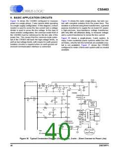
Before AC Gain Calibration (Vgain Register = 1)
250 mV
230 mV
0.9999...
0.92
Figure 14. System Calibration of Gain.
DC Signal
Instantaneous Voltage
Register Values
For gain calibrations, there is an absolute limit on the
RMS voltage levels that are selected for the gain cali-
bration input signals. The maximum value that the gain
registers can attain is 4. Therefore, if the signal level of
the applied input is low enough that it causes the
CS5463 to attempt to set either gain register higher than
4, the gain calibration result will be invalid and all
CS5463 results obtained while performing measure-
ments will be invalid.
INPUT
SIGNAL
0 V
-1.0000...
-250 mV
VRMS Register = 225300 = 0.92
After AC Gain Calibration (Vgain Register changed to approx. 0.65217)
250 mV
0.65217
0.6000
If the channel gain registers are initially set to a gain oth-
er then 1.0, AC gain calibration should be used.
230 mV
DC Signal
INPUT
SIGNAL
Instantaneous Voltage
Register Values
0 V
7.1.3.1 AC Gain Calibration Sequence
The corresponding gain register should be set to 1.0,
unless a different initial gain value is desired. Initiate an
AC gain calibration. The AC gain calibration algorithm
computes the RMS value of the reference signal applied
to the channel inputs. The RMS register value is then di-
vided into 0.6 and the quotient is stored in the corre-
-250 mV
-0.65217
VRMS Register = 0.600000
Figure 16. Example of AC Gain Calibration
shows that a positive (or negative) DC level signal can
be used even though an AC gain calibration is being ex-
ecuted.
sponding
gain
register.
Each
instantaneous
measurement will be multiplied by its corresponding AC
gain value.
DS678PP1
37

 CIRRUS [ CIRRUS LOGIC ]