CS5463
However, an AC signal cannot be used for DC gain cal-
ibration.
can be accomplished by restoring zero to the AC off-
set register and then perform an AC offset calibration
sequence. The adjustment could also be done by
multiplying the AC offset register value that was cal-
culated in step 2 by the gain calculated in step 3 and
updating the AC offset register with the product.
7.1.3.2 DC Gain Calibration Sequence
Initiate a DC gain calibration. The corresponding gain
register is restored to default (1.0). The DC gain calibra-
tion averages the channel’s instantaneous measure-
ments over one computation cycle (N samples). The
average is then divided into 1.0 and the quotient is
stored in the corresponding gain register
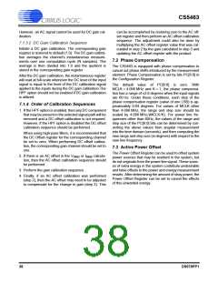
7.2 Phase Compensation
The CS5463 is equipped with phase compensation to
cancel out phase shifts introduced by the measurement
element. Phase Compensation is set by bits PC[6:0] in
the Configuration Register.
After the DC gain calibration, the instantaneous register
will read at full-scale whenever the DC level of the input
signal is equal to the level of the DC calibration signal
applied to the inputs during the DC gain calibration.The
HPF option should not be enabled if DC gain calibration
is utilized.
The default value of PC[6:0] is zero. With
MCLK = 4.096 MHz and K = 1, the phase compensa-
tion has a range of 2.8 degrees when the input signals
are 60 Hz. Under these conditions, each step of the
phase compensation register (value of one LSB) is ap-
proximately 0.04 degrees. For values of MCLK other
than 4.096 MHz, the range and step size should be
scaled by 4.096 MHz/(MCLK/K). For power line fre-
quencies other than 60Hz, the values of the range and
step size of the PC[6:0] bits can be determined by con-
verting the above values from angular measurement
into the time domain (seconds), and then computing the
new range and step size (in degrees) with respect to the
new line frequency.
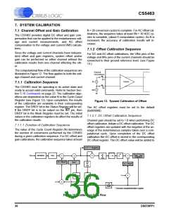
7.1.4 Order of Calibration Sequences
1. If the HPF option is enabled, then any DC component
that may be present in the selected signal path will be
removed and a DC offset calibration is not required.
However, if the HPF option is disabled the DC offset
calibration sequence should be performed.
When using high-pass filters, it is recommended that
the DC Offset register for the corresponding channel
be set to zero. When performing DC offset calibra-
tion, the corresponding gain channel should be set to
one.
7.3 Active Power Offset
The Power Offset Register can be used to offset system
power sources that may be resident in the system, but
do not originate from the power line signal. These sourc-
es of extra energy in the system contribute undesirable
and false offsets to the power and energy measurement
results. After determining the amount of stray power, the
Power Offset Register can be set to cancel the effects
of this unwanted energy.
2. If there is an AC offset in the V
or I
calcula-
RMS
RMS
tion, then the AC offset calibration sequence should
be performed.
3. Perform the gain calibration sequence.
4. Finally, if an AC offset calibration was performed
(step 2), then the AC offset may need to be adjusted
to compensate for the change in gain (step 3). This
38
DS678PP1

 CIRRUS [ CIRRUS LOGIC ]