CS2000-OTP
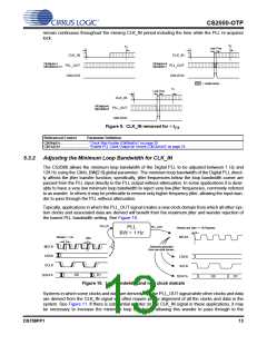
remain continuous throughout the missing CLK_IN period including the time while the PLL re-acquires
lock.
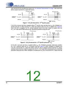
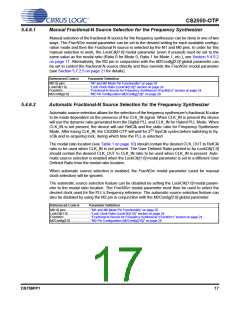
tCS
tCS
Lock Time
CLK_IN
PLL_OUT
UNLOCK
CLK_IN
PLL_OUT
UNLOCK
ClkSkipEn=1
ClkOutUnl=0 or 1
ClkSkipEn=0
ClkOutUnl=1
= invalid clocks
tCS
Lock Time
CLK_IN
PLL_OUT
UNLOCK
ClkSkipEn=0
ClkOutUnl=0
Figure 9. CLK_IN removed for < t
CS
Referenced Control
Parameter Definition
ClkSkipEn..............................“Clock Skip Enable (ClkSkipEn)” on page 25
ClkOutUnl..............................“Enable PLL Clock Output on Unlock (ClkOutUnl)” on page 25
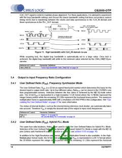
5.3.2
Adjusting the Minimum Loop Bandwidth for CLK_IN
The CS2000 allows the minimum loop bandwidth of the Digital PLL to be adjusted between 1 Hz and
128 Hz using the ClkIn_BW[2:0] global parameter. The minimum loop bandwidth of the Digital PLL direct-
ly affects the jitter transfer function; specifically, jitter frequencies below the loop bandwidth corner are
passed from the PLL input directly to the PLL output without attenuation. In some applications it is desir-
able to have a very low minimum loop bandwidth to reject very low jitter frequencies, commonly referred
to as wander. In others it may be preferable to remove only higher frequency jitter, allowing the input wan-
der to pass through the PLL without attenuation.
Typically, applications in which the PLL_OUT signal creates a new clock domain from which all other sys-
tem clocks and associated data are derived will benefit from the maximum jitter and wander rejection of
the lowest PLL bandwidth setting. See Figure 10.
CLK_IN
PLL_OUT
PLL
Wander and Jitter > 1 Hz Rejected
BW = 1 Hz
MCLK
Wander > 1 Hz
Jitter
MCLK
Subclocks generated
from new clock domain.
or
LRCK
SCLK
LRCK
SCLK
D0
D1
SDATA
D0
D1
SDATA
Figure 10. Low bandwidth and new clock domain
Systems in which some clocks and data are derived from the PLL_OUT signal while other clocks and data
are derived from the CLK_IN signal will often require phase alignment of all the clocks and data in the
system. See Figure 11. If there is substantial wander on the CLK_IN signal in these applications, it may
be necessary to increase the minimum loop bandwidth allowing this wander to pass through to the
DS758PP1
13

 CIRRUS [ CIRRUS LOGIC ]