If over-scale and under-scale limiting is disabled, the PGA
can be used with rail-to-rail voltage output, for example, in
applications that require a 0.5V to 4.5V voltage scale.
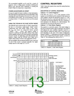
THEORY OF OPERATION
REFERENCE
The XTR108 has an on-board precision bandgap voltage
reference with output at pin 21 (REFOUT). The value of the
reference is factory-trimmed to 1.193V, with a typical tem-
perature drift of 5ppm/°C. Pins 21 (REFOUT) and 20 (REFIN)
must be connected together to use the internal reference.
The PGA uses advanced auto-zero circuit techniques to achieve
high DC precision, and reduce mismatches and errors within
the chip such as input offset, offset temperature drift, and low-
frequency noise (see the input noise typical characteristic).
The basic clock frequency of the auto-zero loop is about
6.5kHz. Due to the switching nature of the auto-zero circuit,
the output of the PGA can have a noticeable clock feed-
through ripple in higher gains. This noise can be reduced by
External circuitry, such as a voltage excited sensor or an
Analog-to-Digital Converter (ADC), can be connected to the
REFOUT pin. The unbuffered REFOUT is capable of sourcing
current but not sinking.
the addition of a 0.01µF capacitor between pin 7 (CFILTER
)
and the local ground, pin 12 (IRET). This creates a one-pole
low-pass filter with –3dB frequency at about 1.5kHz. If
wider bandwidth or faster settling time is needed, the CFILTER
can be reduced or eliminated at the expense of higher glitch
amplitude at the output. Please refer to the typical step
response traces for settling time comparisons.
If the application necessitates, an external reference can be
connected to the XTR108 REFIN pin, as long as the reference
does not exceed 1.4V. The REFIN pin has a high input
impedance with the input current not exceeding a few
nanoamps.
INPUT MULTIPLEXER
ZERO DACS
The XTR108 input multiplexer is a full 6 by (2+2) cross-
point switch. The current references and PGA inputs can be
independently connected to any of the six external pins,
including simultaneous connections to the same pin. This
allows a great flexibility in the sensor excitation and input
configuration. The input pins must not be driven below the
IRET potential or above VS.
Two output-referred, 8-bit Digital-to-Analog Converters
(DACs) (coarse and fine with a pedestal) set the zero level of
the PGA output. They allow setting a desired zero-scale
output level and compensate the initial offset at the PGA input
due to the sensor and resistor mismatches, sensor non-ideali-
ties, etc. Both coarse and fine DACs are bidirectional and
allow the output level to be set above or below a preset
pedestal.
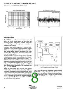
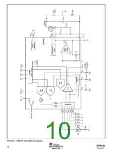
See Figure 2 for an RTD sensor connected to pin VIN0 with
both IREF supplied and PGA VIN+ sensed at that pin. The
other five input pins are used for a bank of RZ resistors that
can be selected during the calibration process for a particular
measurement range.
Output signals of the DACs, IZ COARSE and IZ FINE, are
summed with the pedestal, IZ PROGRAM. Each of the DACs
has 8-bit resolution (256 steps) with 4-bit overlap between
the coarse and fine DACs. This means that one LSB of the
coarse DAC is equal to 16 fine LSBs, and the full-scale
range of the fine DAC is equal to 16 coarse LSBs. This
effectively produces 12-bit adjustment resolution.
PROGRAMMABLE GAIN
INSTRUMENTATION AMPLIFIER
The programmable gain instrumentation amplifier has seven
voltage-gain settings in binary steps from 6.25V/V to 400V/V.
The input common-mode range of the PGA is 0.2V to 3.5V
above the IRET potential.
This overlap allows the user to set pre-calculated values
before the calibration, using the coarse DAC only and adjust
the zero output level with the fine DAC during the calibra-
tion process see Table II for the equations for calculating the
value of the output when zero differential voltage is applied
at the PGA input. For the adjustment range, LSB sizes, and
linearity values of the Zero DACs, please refer to the
electrical characteristics table.
Normally, in the application for 4-20mA transmitters, the
PGA output voltage range should be set to VZERO = 0.5V and
VFS = 2.5V. Connecting a resistor (RVI = 6.34kΩ) between
pin 9 (VO) and pin 10 (IIN) converts this voltage to the signal
for the output amplifier that produces a 4-20mA scale
current output. In this mode, the PGA voltage gain converts
to an overall transconductance in the range of 50mA/V to
3200mA/V (approximately). Table I shows the gain to
transconductance relationship.
Note that a DAC can be set to a value that produces an
output below the under-scale level. In this case, the under-
scale limit will prevent the output from getting to the desired
value. The value of the minimum scale should not be set so
low that the PGA voltage output, VO, goes below its speci-
fied range of 0.2V from IRET
.
VOLTAGE GAIN
6.25 12.5 25
50 100 200 400
V/V
ADJUSTABLE OVER-SCALE AND
UNDER-SCALE LIMITING CIRCUIT
OUTPUT TRANSCONDUCTANCE 49 99 197 394 789 1577 3155
mA/V
The XTR108 incorporates circuitry to set adjustable limits at
the output in cases when the sensor signal goes above or
below its range. There are 16 levels for over-scale limit
adjustment (4-bit DAC) and 8 levels for the under-scale (3-bit
DAC).
FULL-SCALE DIFFERENTIAL VIN 320 160 80
40
20
10
5
mV
TABLE I. PGA Gain, Corresponding Loop Transductance
and Input Full-Scale Differential Voltage.
XTR108
SBOS187C
9
www.ti.com

 BB [ BURR-BROWN CORPORATION ]