PCM1804
SLES022A – DECEMBER 2001
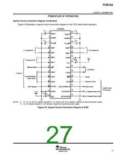
APPLICATION INFORMATION
board design and layout considerations
V
, V
pins
CC DD
The digital and analog power supply lines to the PCM1804 should be bypassed to the corresponding ground
pins with 0.1-µF ceramic and 10-µF tantalum capacitors placed as close to the pins as possible to maximize
the dynamic performance of the ADC. Although the PCM1804 has two power lines to maximize the potential
of dynamic performance, using one common power supply is recommended to avoid unexpected power supply
trouble like latch-up or power-supply sequence.
V
V
pins
IN
Use 100-pF ceramic capacitors between V L+, V L–, V R+, V R–, and AGND, and 0.022-µF ceramic
capacitors between V L+ and V L–, V R+, and V R– to remove higher-frequency noise at the delta-sigma
input section.
IN
IN
IN
IN
IN
IN
IN
IN
, V inputs
REFX COMX
Use 0.1-µF ceramic and 10-µF tantalum capacitors between V
insurelow-sourceimpedanceatADCreferences.Use0.1-µFtantalumcapacitorsbetweenV
L, V
R, and corresponding AGNDx, to
REF
REF
L,V
Rand
COM
COM
corresponding AGNDx to insure low-source impedance of common voltage. These capacitors should be
located as close as possible to the V L, V R, V L, and V R pins to reduce dynamic errors on
REF
REF
COM
COM
references and common voltage. The dc voltage level of these pins is 2.5 V.
DATA/DSDR, BCK/DSDL, and LRCK/DSDBCK pins
The DATA/DSDR, BCK/DSDL, and LRCK/DSDBCK pins in master mode have large load drive capability.
Locating the buffer near the PCM1804 and minimizing the load capacitance, minimizes the digital analog
crosstalk and maximizes the dynamic performance of the ADC.
system clock
The quality of the system clock may influence dynamic performance, as the PCM1804 operates based on
system clock. In that case, it may be required to consider the system clock duty, jitter, and the time difference
between system clock transition and BCK/DSDL or LRCK/DSDBCK transition in slave mode.
reset control
If capacitors larger than 10 µF are used on V
L and V
R, the external reset control with a delay time
REF
REF
corresponding to the V
L and V
R response is required. Also, it works as a power-down control.
REF
REF
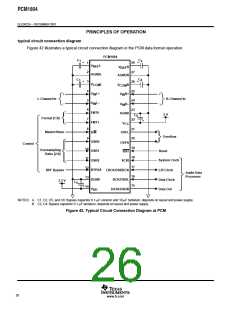
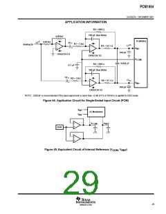
application circuit for single-end input
An application circuit for a single-end input circuit is shown in Figure 44. The maximum signal input voltage and
differential gain of this circuit is designed as Vinmax = 8.28 Vpp, A = 0.3. Differential gain (Ad) is given by
R3/R1(R4/R2) as normal inverted gain amp. Resistor R5 (R6) in the feedback loop gives low-impedance drive
operation and noise filtering for analog input of the PCM1804. The circuit technique R5 (R6) is recommended.
28
www.ti.com

 BB [ BURR-BROWN CORPORATION ]