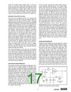
sider the unity gain stable voltage feedback OPA680, since
the feedback resistor is the compensation element for a
current feedback op amp. Wideband inverting operation
(and especially summing) is particularly suited to the
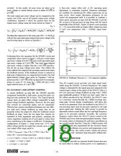
OPA681. Figure 8 shows a typical inverting configuration
where the I/O impedances and signal gain from Figure 1 are
retained in an inverting circuit configuration.
ground on the non-inverting input to achieve bias current
error cancellation at the output. The input bias currents for
a current feedback op amp are not generally matched in
either magnitude or polarity. Connecting a resistor to ground
on the non-inverting input of the OPA681 in the circuit of
Figure 8 will actually provide additional gain for that input’s
bias and noise currents, but will not decrease the output DC
error since the input bias currents are not matched.
OUTPUT CURRENT AND VOLTAGE
+5V
The OPA681 provides output voltage and current capabili-
ties that are unsurpassed in a low cost monolithic op amp.
Under no-load conditions at 25°C, the output voltage typi-
cally swings closer than 1V to either supply rail; the guaran-
teed swing limit is within 1.2V of either rail. Into a 15Ω load
(the minimum tested load), it is guaranteed to deliver more
than ±135mA.
Power supply
de-coupling
not shown
50Ω Load
DIS
VO
50Ω
OPA681
50Ω
Source
RG
182Ω
RF
365Ω
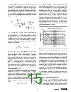
The specifications described above, though familiar in the
industry, consider voltage and current limits separately. In
many applications, it is the voltage x current, or V-I product,
which is more relevant to circuit operation. Refer to the
“Output Voltage and Current Limitations” plot in the Typi-
cal Performance Curves. The X and Y axes of this graph
show the zero-voltage output current limit and the zero-
current output voltage limit, respectively. The four quad-
rants give a more detailed view of the OPA681’s output
drive capabilities, noting that the graph is bounded by a
“Safe Operating Area” of 1W maximum internal power
dissipation. Superimposing resistor load lines onto the plot
shows that the OPA681 can drive ±2.5V into 25Ω or ±3.5V
into 50Ω without exceeding the output capabilities or the
1W dissipation limit. A 100Ω load line (the standard test
circuit load) shows the full ±3.9V output swing capability,
as shown in the Typical Specifications.
VI
RM
68.1Ω
–5V
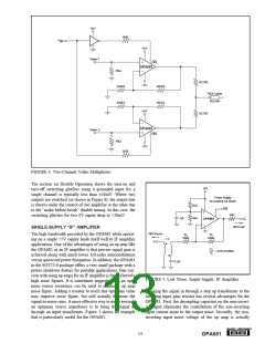
FIGURE 8. Inverting Gain of –2 with Impedance Matching.
In the inverting configuration, two key design consider-
ations must be noted. The first is that the gain resistor (RG)
becomes part of the signal channel input impedance. If input
impedance matching is desired (which is beneficial when-
ever the signal is coupled through a cable, twisted pair, long
PC board trace or other transmission line conductor), it is
normally necessary to add an additional matching resistor to
ground. RG by itself is normally not set to the required input
impedance since its value, along with the desired gain, will
determine an RF which may be non-optimal from a fre-
quency response standpoint. The total input impedance for
the source becomes the parallel combination of RG and RM.
The minimum specified output voltage and current over
temperature are set by worst-case simulations at the cold
temperature extreme. Only at cold startup will the output
current and voltage decrease to the numbers shown in the
guaranteed tables. As the output transistors deliver power,
their junction temperatures will increase, decreasing their
VBE’s (increasing the available output voltage swing) and
increasing their current gains (increasing the available out-
put current). In steady-state operation, the available output
voltage and current will always be greater than that shown
in the over-temperature specifications since the output stage
junction temperatures will be higher than the minimum
specified operating ambient.
The second major consideration, touched on in the previous
paragraph, is that the signal source impedance becomes part
of the noise gain equation and will have slight effect on the
bandwidth through Equation 1. The values shown in Figure
8 have accounted for this by slightly decreasing RF (from
Figure 1) to re-optimize the bandwidth for the noise gain of
Figure 8 (NG = 2.74) In the example of Figure 8, the RM
value combines in parallel with the external 50Ω source
impedance, yielding an effective driving impedance of
50Ω || 68Ω = 28.8Ω. This impedance is added in series with
RG for calculating the noise gain—which gives NG = 2.74.
This value, along with the RF of Figure 8 and the inverting
input impedance of 41Ω, are inserted into Equation 3 to get
a feedback transimpedance nearly equal to the 484Ω opti-
mum value.
To maintain maximum output stage linearity, no output
short-circuit protection is provided. This will not normally
be a problem since most applications include a series match-
ing resistor at the output that will limit the internal power
dissipation if the output side of this resistor is shorted to
ground. However, shorting the output pin directly to the
adjacent positive power supply pin (8-pin packages) will, in
most cases, destroy the amplifier. If additional short-circuit
protection is required, consider a small series resistor in the
power supply leads. This will, under heavy output loads,
Note that the non-inverting input in this bipolar supply
inverting application is connected directly to ground. It is
often suggested that an additional resistor be connected to
®
16
OPA681

 BB [ BURR-BROWN CORPORATION ]