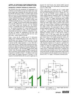
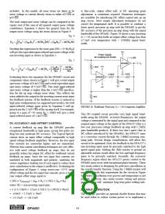
attenuated if reflected to the input side of RG. Using the 1:2
(turns ratio) step-up transformer reflects the 50Ω source imped-
ance at the primary through to the secondary as a 200Ω source
impedance (and the 200Ω RG resistor is reflected through to the
transformer primary as a 50Ω input matching impedance). The
noise gain (NG) to the amplifier output is then 1+ 600/400 =
2.5V/V. Taking the op amp’s 2.2nV/√Hz input voltage noise
times this noise gain to the output, then reflecting this noise
term to the input side of the RG resistor, divides it by 3. This
gives a net gain of 0.833 for the non-inverting input voltage
noise when reflected to the input point for the op amp circuit.
This is further reduced when referred back to the transformer
primary.
or as one model on a disk from the Burr-Brown Applications
department (1-800-548-6132). The Applications department
is also available for design assistance at this number. These
models do a good job of predicting small-signal AC and
transient performance under a wide variety of operating
conditions. They do not do as well in predicting the har-
φ
monic distortion or dG/d characteristics. These models do
not attempt to distinguish between the package types in their
small-signal AC performance.
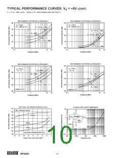
OPERATING SUGGESTIONS
SETTING RESISTOR VALUES TO
OPTIMIZE BANDWIDTH
The relatively low gain IF amplifier circuit of Figure 5 gives a
12dB noise figure at the input of the transformer. Increasing the
RF resistor to 600Ω (once RG is set to 200Ω for input impedance
matching) will slightly reduce the bandwidth. Measured results
show 150MHz small-signal bandwidth for the circuit of Figure
5 with exceptional flatness through 30MHz. Although the
OPA681 does not show an intercept characteristic for the
2-tone, 3rd-order intermodulation distortion, it does hold a very
high spurious free dynamic range through high output powers
and frequencies. The maximum single-tone power at the match-
ed load for the single-supply circuit of Figure 5 is 1dBm (this
requires a 2.8Vp-p swing at the output pin of the OPA681 for
the 2-tone envelope). Measured 2-tone SFDR at this maximum
load power for the circuit of Figure 5 exceeds 55dBc for
frequencies to 30MHz.
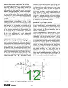
A current feedback op amp like the OPA681 can hold an almost
constant bandwidth over signal gain settings with the proper
adjustment of the external resistor values. This is shown in the
Typical Performance Curves; the small-signal bandwidth de-
creases only slightly with increasing gain. Those curves also
show that the feedback resistor has been changed for each gain
setting. The resistor “values” on the inverting side of the circuit
for a current feedback op amp can be treated as frequency
response compensation elements while their “ratios” set the
signal gain. Figure 6 shows the small-signal frequency response
analysis circuit for the OPA681.
VI
α
DESIGN-INTOOLS
VO
DEMONSTRATION BOARDS
RI
Several PC boards are available to assist in the initial
evaluation of circuit performance using the OPA681 in its
three package styles. All of these are available free as an
unpopulated PC board delivered with descriptive documen-
tation. The summary information for these boards is shown
in the table below.
Z(S) iERR
iERR
RF
RG
BOARD
PART
NUMBER
LITERATURE
REQUEST
NUMBER
FIGURE 6. Current Feedback Transfer Function Analysis
Circuit.
PRODUCT
PACKAGE
OPA681P
OPA681U
OPA681N
8-Pin DIP
8-Pin SO-8
6-Lead SOT23-6 DEM-OPA68xN
DEM-OPA68xP
DEM-OPA68xU
MKT-350
MKT-351
MKT-348
The key elements of this current feedback op amp model are:
α → Buffer gain from the non-inverting input to the inverting input
RI → Buffer output impedance
Contact the Burr-Brown applications support line to request
any of these boards.
iERR → Feedback error current signal
Z(s) → Frequency dependent open loop transimpedance gain from iERR to VO
MACROMODELS AND APPLICATIONS SUPPORT
The buffer gain is typically very close to 1.00 and is
normally neglected from signal gain considerations. It will,
however, set the CMRR for a single op amp differential
amplifier configuration. For a buffer gain α < 1.0, the
CMRR = –20 x log (1– α) dB.
Computer simulation of circuit performance using SPICE is
often useful when analyzing the performance of analog
circuits and systems. This is particularly true for video and
RF amplifier circuits where parasitic capacitance and induc-
tance can have a major effect on circuit performance. A
SPICE model for the OPA681 is available through either the
Burr-Brown Internet web page (http://www.burr-brown.com)
RI, the buffer output impedance, is a critical portion of the
bandwidth control equation. The OPA681 is typically about
41Ω.
®
14
OPA681

 BB [ BURR-BROWN CORPORATION ]