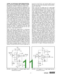
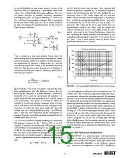
As the desired signal gain increases, this equation will
eventually predict a negative RF. A somewhat subjective
limit to this adjustment can also be set by holding RG to a
minimum value of 20Ω. Lower values will load both the
buffer stage at the input and the output stage if RF gets too
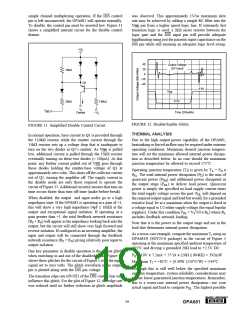
low—actually decreasing the bandwidth. Figure 7 shows the
recommended RF vs NG for both ±5V and a single +5V
operation. The values for RF versus gain shown here are
approximately equal to the values used to generate the
Typical Performance Curves. They differ in that the opti-
mized values used in the Typical Performance Curves are
also correcting for board parasitics not considered in the
simplified analysis leading to Equation 3. The values shown
in Figure 7 give a good starting point for design where
bandwidth optimization is desired.
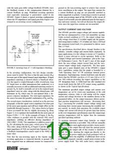
A current feedback op amp senses an error current in the
inverting node (as opposed to a differential input error
voltage for a voltage feedback op amp) and passes this on to
the output through an internal frequency dependent
transimpedance gain. The Typical Performance Curves show
this open-loop transimpedance response. This is analogous
to the open-loop voltage gain curve for a voltage feedback
op amp. Developing the transfer function for the circuit of
Figure 6 gives Equation 1:
Eq. 1
RF
α 1+
RG
RF + RI 1+
Z(S)
VO
VI
α NG
RF + RI NG
=
=
RF
RG
1+
Z(S)
1+
RF
NG = 1+
RG
FEEDBACK RESISTOR vs NOISE GAIN
600
500
This is written in a loop gain analysis format where the
errors arising from a non-infinite open-loop gain are shown
in the denominator. If Z(s) were infinite over all frequencies,
the denominator of Equation 1 would reduce to 1 and the
ideal desired signal gain shown in the numerator would be
achieved. The fraction in the denominator of Equation 1
determines the frequency response. Equation 2 shows this as
the loop gain equation:
+5V
400
300
200
±5V
100
0
Eq. 2
0
5
10
15
20
Z(S)
Noise Gain
= Loop Gain
RF + RI NG
FIGURE 7. Recommended Feedback Resistor vs Noise Gain.
If 20 x log (RF + NG x RI) were drawn on top of the open-
loop transimpedance plot, the difference between the two
would be the loop gain at a given frequency. Eventually,
Z(s) rolls off to equal the denominator of Equation 2 at
which point the loop gain has reduced to 1 (and the curves
have intersected). This point of equality is where the
amplifier’s closed-loop frequency response given by Equa-
tion 1 will start to roll off, and is exactly analogous to the
frequency at which the noise gain equals the open-loop
voltage gain for a voltage feedback op amp. The difference
here is that the total impedance in the denominator of
Equation 2 may be controlled somewhat separately from the
desired signal gain (or NG).
The total impedance going into the inverting input may be
used to adjust the closed-loop signal bandwidth. Inserting a
series resistor between the inverting input and the summing
junction will increase the feedback impedance (denominator
of Equation 2), decreasing the bandwidth. This approach to
bandwidth control is used for the inverting summing circuit
on the front page. The internal buffer output impedance for
the OPA681 is slightly influenced by the source impedance
looking out of the non-inverting input terminal. High source
resistors will have the effect of increasing RI, decreasing the
bandwidth. For those single-supply applications which de-
velop a midpoint bias at the non-inverting input through
high valued resistors, the decoupling capacitor is essential
for power supply noise rejection, non-inverting input noise
current shunting, and to minimize the high frequency value
for RI in Figure 6.
The OPA681 is internally compensated to give a maximally
flat frequency response for RF = 402Ω at NG = 2 on ±5V
supplies. Evaluating the denominator of Equation 2 (which
is the feedback transimpedance) gives an optimal target of
484Ω. As the signal gain changes, the contribution of the
NG x RI term in the feedback transimpedance will change,
but the total can be held constant by adjusting RF. Equation
3 gives an approximate equation for optimum RF over signal
gain:
INVERTING AMPLIFIER OPERATION
Since the OPA681 is a general purpose, wideband current
feedback op amp, most of the familiar op amp application
circuits are available to the designer. Those applications that
require considerable flexibility in the feedback element
(e.g., integrators, transimpedance, some filters) should con-
RF = 484Ω – NG RI
Eq. 3
®
15
OPA681

 BB [ BURR-BROWN CORPORATION ]