reduce the available output voltage swing. A 5Ω series
resistor in each power supply lead will limit the internal
power dissipation to less than 1W for an output short circuit
while decreasing the available output voltage swing only
0.5V for up to 100mA desired load currents. Always place
the 0.1µF power supply decoupling capacitors after these
supply current limiting resistors directly on the supply pins.
In most op amps, increasing the output voltage swing in-
creases harmonic distortion directly. The Typical Perfor-
mance Curves show the 2nd harmonic increasing at a little
less than the expected 2X rate while the 3rd harmonic
increases at a little less than the expected 3X rate. Where the
test power doubles, the difference between it and the 2nd
harmonic decreases less than the expected 6dB while the
difference between it and the 3rd decreases by less than the
expected 12dB. This also shows up in the 2-tone, 3rd-order
intermodulation spurious (IM3) response curves. The 3rd-
order spurious levels are extremely low at low output power
levels. The output stage continues to hold them low even as
the fundamental power reaches very high levels. As the
Typical Performance Curves show, the spurious
intermodulation powers do not increase as predicted by a
traditional intercept model. As the fundamental power level
increases, the dynamic range does not decrease significantly.
For two tones centered at 20MHz, with 10dBm/tone into a
matched 50Ω load (i.e., 2Vp-p for each tone at the load,
which requires 8Vp-p for the overall 2-tone envelope at the
output pin), the Typical Performance Curves show 62dBc
difference between the test-tone power and the 3rd-order
intermodulation spurious levels. This exceptional perfor-
mance improves further when operating at lower frequen-
cies.
DRIVING CAPACITIVE LOADS
One of the most demanding and yet very common load
conditions for an op amp is capacitive loading. Often, the
capacitive load is the input of an A/D converter—including
additional external capacitance which may be recommended
to improve A/D linearity. A high speed, high open-loop gain
amplifier like the OPA681 can be very susceptible to de-
creased stability and closed-loop response peaking when a
capacitive load is placed directly on the output pin. When
the amplifier’s open-loop output resistance is considered,
this capacitive load introduces an additional pole in the
signal path that can decrease the phase margin. Several
external solutions to this problem have been suggested.
When the primary considerations are frequency response
flatness, pulse response fidelity and/or distortion, the sim-
plest and most effective solution is to isolate the capacitive
load from the feedback loop by inserting a series isolation
resistor between the amplifier output and the capacitive
load. This does not eliminate the pole from the loop re-
sponse, but rather shifts it and adds a zero at a higher
frequency. The additional zero acts to cancel the phase lag
from the capacitive load pole, thus increasing the phase
margin and improving stability.
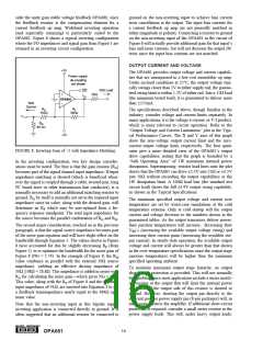
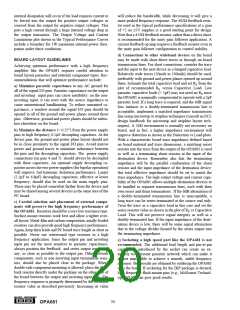
NOISE PERFORMANCE
Wideband current feedback op amps generally have a higher
output noise than comparable voltage feedback op amps.
The OPA681 offers an excellent balance between voltage
and current noise terms to achieve low output noise. The
inverting current noise (15pA/√Hz) is significantly lower
than earlier solutions while the input voltage noise
(2.2nV/√Hz) is lower than most unity gain stable, wideband,
voltage feedback op amps. This low input voltage noise was
achieved at the price of higher non-inverting input current
noise (12pA/√Hz). As long as the AC source impedance
looking out of the non-inverting node is less than 100Ω, this
current noise will not contribute significantly to the total
output noise. The op amp input voltage noise and the two
input current noise terms combine to give low output noise
under a wide variety of operating conditions. Figure 9 shows
the op amp noise analysis model with all the noise terms
The Typical Performance Curves show the recommended
RS vs Capacitive Load and the resulting frequency response
at the load. Parasitic capacitive loads greater than 2pF can
begin to degrade the performance of the OPA681. Long PC
board traces, unmatched cables, and connections to multiple
devices can easily cause this value to be exceeded. Always
consider this effect carefully, and add the recommended
series resistor as close as possible to the OPA681 output pin
(see Board Layout Guidelines).
DISTORTION PERFORMANCE
The OPA681 provides good distortion performance into a
100Ω load on ±5V supplies. Relative to alternative solu-
tions, it provides exceptional performance into lighter loads
and/or operating on a single +5V supply. Generally, until the
fundamental signal reaches very high frequency or power
levels, the 2nd harmonic will dominate the distortion with a
negligible 3rd harmonic component. Focusing then on the
2nd harmonic, increasing the load impedance improves
distortion directly. Remember that the total load includes the
feedback network—in the non-inverting configuration (Fig-
ure 1) this is the sum of RF + RG, while in the inverting
configuration it is just RF. Also, providing an additional
supply de-coupling capacitor (0.1µF) between the supply
pins (for bipolar operation) improves the 2nd-order distor-
tion slightly (3dB to 6dB).
ENI
EO
OPA681
RS
IBN
ERS
RF
√4kTRS
√4kTRF
IBI
RG
4kT
RG
4kT = 1.6E –20J
at 290°K
FIGURE 9. Op Amp Noise Analysis Model.
®
17
OPA681

 BB [ BURR-BROWN CORPORATION ]