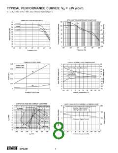
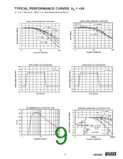
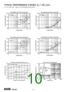
SINGLE-SUPPLY A/D CONVERTER INTERFACE
impedance looking into the inverting input from the sum-
ming junction (see Setting Resistor Values to Optimize
Performance section). Using 100Ω feedback (to get a signal
gain of –2 from each input to the output pin) requires an
additional 20Ω in series with the inverting input to increase
the feedback impedance. With this resistor added to the
typical internal RI = 41Ω, the total feedback impedance is
100Ω + (65Ω x 6) = 490Ω, which is equal to the required
value to get a maximum bandwidth flat frequency response
for NG = 6. Tested performance shows more than 200MHz
small signal bandwidth and a –1dBm compression of 15dBm
at the matched 50Ω load through 100MHz.
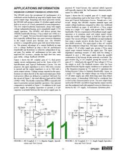
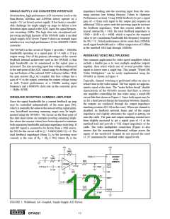
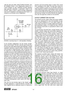
Most modern, high performance A/D converters (such as the
Burr-Brown ADS8xx and ADS9xx series) operate on a
single +5V (or lower) power supply. It has been a consider-
able challenge for single-supply op amps to deliver a low
distortion input signal at the ADC input for signal frequen-
cies exceeding 5MHz. The high slew rate, exceptional out-
put swing and high linearity of the OPA681 make it an ideal
single-supply ADC driver. Figure 3 shows an example input
interface to a very high performance 10-bit, 60MSPS CMOS
converter.
The OPA681 in the circuit of Figure 3 provides > 180MHz
bandwidth operating at a signal gain of +4 with a 2Vp-p
output swing. One of the primary advantages of the current
feedback internal architecture used in the OPA681 is that
high bandwidth can be maintained as the signal gain is
increased. The non-inverting input bias voltage is referenced
to the mid-point of the ADC signal range by dividing off the
top and bottom of the internal ADC reference ladder. With
the gain resistor (RG) AC-coupled, this bias voltage has a
gain of +1 to the output, centering the output voltage swing
as well. Tested performance at a 20MHz analog input
frequency and a 60MSPS clock rate on the converter gives
> 58dBc SFDR.
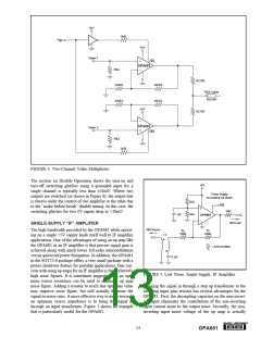
WIDEBAND VIDEO MULTIPLEXING
One common application for video speed amplifiers which
include a disable pin is to wire multiple amplifier outputs
together, then select which one of several possible video
inputs to source onto a single line. This simple “Wired-OR
Video Multiplexer” can be easily implemented using the
OPA681 as shown in Figure 4.
Typically, channel switching is performed either on sync or
retrace time in the video signal. The two inputs are approxi-
mately equal at this time. The “make-before-break” disable
characteristic of the OPA681 ensures that there is always
one amplifier controlling the line when using a wired-OR
circuit like that shown in Figure 4. Since both inputs may be
on for a short period during the transition between channels,
the outputs are combined through the output impedance
matching resistors (82.5Ω in this case). When one channel is
disabled, its feedback network forms part of the output
impedance and slightly attenuates the signal in getting out
onto the cable. The gain and output matching resistor have
been slightly increased to get a signal gain of +1 at the
matched load and provide a 75Ω output impedance to the
cable. The video multiplexer connection (Figure 4) also
insures that the maximum differential voltage across the
inputs of the unselected channel do not exceed the rated
±1.2V maximum for standard video signal levels.
WIDEBAND INVERTING SUMMING AMPLIFIER
Since the signal bandwidth for a current feedback op amp
may be controlled independently of the noise gain (NG,
which is normally the same as the non-inverting signal gain),
very broadband inverting summing stages may be imple-
mented using the OPA681. The circuit on the front page of
this data sheet shows an example inverting summing ampli-
fier where the resistor values have been adjusted to maintain
both maximum bandwidth and input impedance matching. If
each RF signal is assumed to be driven from a 50Ω source,
the NG for this circuit will be (1 + 100Ω/(100Ω/5)) = 6. The
total feedback impedance (from VO to the inverting error
current) is the sum of RF + (RI x NG) where RI is the
+5V
RF
+5V
360Ω
RG
120Ω
Clock
ADS823
10-Bit
60MSPS
0.1µF
50Ω
Input
Input
OPA681
2Vp-p
22pF
0.5Vp-p
0.1µF
CM
DIS
2kΩ
2kΩ
+3.5V
REFT
0.1µF
+2.5V DC Bias
+1.5V
REFB
0.1µF
FIGURE 3. Wideband, AC-Coupled, Single-Supply A/D Driver.
®
12
OPA681

 BB [ BURR-BROWN CORPORATION ]