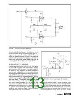
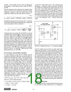
simple channel multiplexing operation. If the DIS control
pin is left unconnected, the OPA681 will operate normally.
To disable, the control pin must be asserted low. Figure 11
shows a simplified internal circuit for the disable control
feature.
was observed. This approximately 1V/ns maximum slew
rate may be achieved by adding a simple RC filter into the
VDIS pin from a higher speed logic line. If extremely fast
transition logic is used, a 2kΩ series resistor between the
logic gate and the DIS input pin will provide adequate
bandlimiting using just the parasitic input capacitance on the
DIS pin while still ensuring an adequate logic level swing.
+VS
40
20
Output Voltage
(0V Input)
15kΩ
0
–20
–40
Q1
4.8V
VDIS
0.2V
25kΩ
110kΩ
IS
VDIS
Time (20ns/div)
Control
–VS
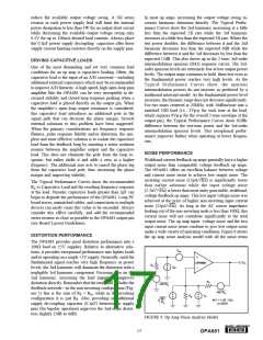
FIGURE 12. Disable/Enable Glitch.
FIGURE 11. Simplified Disable Control Circuit.
THERMAL ANALYSIS
In normal operation, base current to Q1 is provided through
the 110kΩ resistor while the emitter current through the
15kΩ resistor sets up a voltage drop that is inadequate to
turn on the two diodes in Q1’s emitter. As VDIS is pulled
low, additional current is pulled through the 15kΩ resistor
eventually turning on these two diodes (≈ 100µA). At this
point, any further current pulled out of VDIS goes through
those diodes holding the emitter-base voltage of Q1 at
approximately zero volts. This shuts off the collector current
out of Q1, turning the amplifier off. The supply current in
the disable mode are only those required to operate the
circuit of Figure 11. Additional circuitry ensures that turn-on
time occurs faster than turn-off time (make-before-break).
Due to the high output power capability of the OPA681,
heatsinking or forced airflow may be required under extreme
operating conditions. Maximum desired junction tempera-
ture will set the maximum allowed internal power dissipa-
tion as described below. In no case should the maximum
junction temperature be allowed to exceed 175°C.
Operating junction temperature (TJ) is given by TA + PD x
θJA. The total internal power dissipation (PD) is the sum of
quiescent power (PDQ) and additional power dissipated in
the output stage (PDL) to deliver load power. Quiescent
power is simply the specified no-load supply current times
the total supply voltage across the part. PDL will depend on
the required output signal and load but would, for a grounded
resistive load, be at a maximum when the output is fixed at
a voltage equal to 1/2 either supply voltage (for equal bipolar
When disabled, the output and input nodes go to a high
impedance state. If the OPA681 is operating in a gain of +1,
this will show a very high impedance (4pF || 1MΩ) at the
output and exceptional signal isolation. If operating at a
gain greater than +1, the total feedback network resistance
(RF + RG) will appear as the impedance looking back into the
output, but the circuit will still show very high forward and
reverse isolation. If configured as an inverting amplifier, the
input and output will be connected through the feedback
network resistance (RF + RG) giving relatively poor input to
output isolation.
2
supplies). Under this condition PDL = VS /(4 x RL) where RL
includes feedback network loading.
Note that it is the power in the output stage and not in the
load that determines internal power dissipation.
As a worst-case example, compute the maximum TJ using an
OPA681N (SOT23-6 package) in the circuit of Figure 1
operating at the maximum specified ambient temperature of
+85°C and driving a grounded 20Ω load to +2.5V DC:
One key parameter in disable operation is the output glitch
when switching in and out of the disabled mode. Figure 12
shows these glitches for the circuit of Figure 1 with the input
signal set to zero volts. The glitch waveform at the output
pin is plotted along with the DIS pin voltage.
PD = 10V x 7.2mA + 52/(4 x (20Ω || 804Ω)) = 392mW
Maximum TJ = +85°C + (0.39W (150°C/W) = 144°C
Although this is still well below the specified maximum
junction temperature, system reliability considerations may
require lower guaranteed junction temperatures. Remember,
this is a worst-case internal power dissipation—use your
actual signal and load to compute PDL. The highest possible
The transition edge rate (dV/dT) of the DIS control line will
influence this glitch. For the plot of Figure 12, the edge rate
was reduced until no further reduction in glitch amplitude
®
19
OPA681

 BB [ BURR-BROWN CORPORATION ]