included. In this model, all noise terms are taken to be
noise voltage or current density terms in either nV/√Hz or
pA/√Hz.
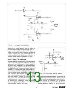
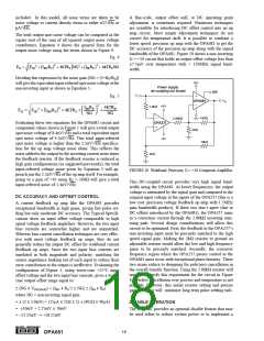
A fine-scale, output offset null, or DC operating point
adjustment, is sometimes required. Numerous techniques
are available for introducing DC offset control into an op
amp circuit. Most simple adjustment techniques do not
correct for temperature drift. It is possible to combine a
lower speed, precision op amp with the OPA681 to get the
DC accuracy of the precision op amp along with the signal
bandwidth of the OPA681. Figure 10 shows a non-inverting
G = +10 circuit that holds an output offset voltage less than
±7.5mV over temperature with > 150MHz signal band-
width.
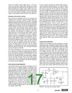
The total output spot noise voltage can be computed as the
square root of the sum of all squared output noise voltage
contributors. Equation 4 shows the general form for the
output noise voltage using the terms shown in Figure 9.
Eq. 4
2
2
2
EO
=
ENI + IBNRS + 4kTRS NG2 + IBIRF + 4kTRFNG
(
)
(
)
(
)
Dividing this expression by the noise gain (NG = (1+RF/RG))
will give the equivalent input-referred spot noise voltage at the
non-inverting input as shown in Equation 5.
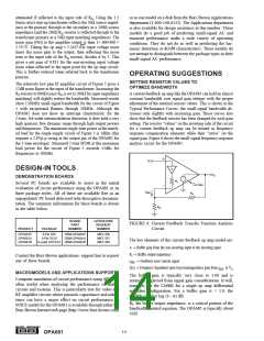
+5V
Power supply
de-coupling not shown
DIS
VI
Eq. 5
VO
OPA681
2
+5V
1.8kΩ
IBIRF
NG
4kTRF
NG
2
2
EN
=
ENI + IBNRS + 4kTRS +
+
(
)
180Ω
2.86kΩ
–5V
Evaluating these two equations for the OPA681 circuit and
component values shown in Figure 1 will give a total output
spot noise voltage of 8.4nV/√Hz and a total equivalent input
spot noise voltage of 4.2nV/√Hz. This total input-referred
spot noise voltage is higher than the 2.2nV/√Hz specifica-
tion for the op amp voltage noise alone. This reflects the
noise added to the output by the inverting current noise times
the feedback resistor. If the feedback resistor is reduced in
high gain configurations (as suggested previously), the total
input-referred voltage noise given by Equation 5 will ap-
proach just the 2.2nV/√Hz of the op amp itself. For example,
going to a gain of +10 using RF = 180Ω will give a total
input-referred noise of 2.4nV/√Hz .
OPA237
20Ω
–5V
18kΩ
2kΩ
FIGURE 10. Wideband, Precision, G = +10 Composite Amplifier.
This DC-coupled circuit provides very high signal band-
width using the OPA681. At lower frequencies, the output
voltage is attenuated by the signal gain and compared to the
original input voltage at the inputs of the OPA237 (this is a
low cost, precision voltage feedback op amp with 1.5MHz
gain bandwidth product). If these two don’t agree (due to
DC offsets introduced by the OPA681), the OPA237 sums
in a correction current through the 2.86kΩ inverting sum-
ming path. Several design considerations will allow this
circuit to be optimized. First, the feedback to the OPA237’s
non-inverting input must be precisely matched to the high
speed signal gain. Making the 2kΩ resistor to ground an
adjustable resistor would allow the low and high frequency
gains to be precisely matched. Secondly, the crossover
frequency region where the OPA237 passes control to the
OPA681 must occur with exceptional phase linearity. These
two issues reduce to designing for pole/zero cancellation in
the overall transfer function. Using the 2.86kΩ resistor will
nominally satisfy this requirement for the circuit in Figure
10. Perfect cancellation over process and temperature is not
possible. However, this initial resistor setting and precise
gain matching will minimize long term pulse settling tails.
DC ACCURACY AND OFFSET CONTROL
A current feedback op amp like the OPA681 provides
exceptional bandwidth in high gains, giving fast pulse set-
tling but only moderate DC accuracy. The Typical Specifi-
cations show an input offset voltage comparable to high
speed voltage feedback amplifiers. However, the two input
bias currents are somewhat higher and are unmatched.
Whereas bias current cancellation techniques are very effec-
tive with most voltage feedback op amps, they do not
generally reduce the output DC offset for wideband current
feedback op amps. Since the two input bias currents are
unrelated in both magnitude and polarity, matching the
source impedance looking out of each input to reduce their
error contribution to the output is ineffective. Evaluating the
configuration of Figure 1, using worst-case +25°C input
offset voltage and the two input bias currents, gives a worst-
case output offset range equal to:
± (NG x VOS(MAX)) + (IBN x RS/2 x NG) ± (IBI x RF)
where NG = non-inverting signal gain
= ± (2 x 5.0mV) + (55µA x 25Ω x 2) ± (402Ω x 40µA)
= ±10mV + 2.75mV ± 16mV
DISABLE OPERATION
The OPA681 provides an optional disable feature that may
be used either to reduce system power or to implement a
= –23.25mV → +28.25mV
®
18
OPA681

 BB [ BURR-BROWN CORPORATION ]