practical PC board layouts, this optional added capacitor
will typically improve the 2nd harmonic distortion perfor-
mance by 3dB to 6dB.
APPLICATIONS INFORMATION
WIDEBAND CURRENT FEEDBACK OPERATION
The OPA681 gives the exceptional AC performance of a
wideband current feedback op amp with a highly linear, high
power output stage. Requiring only 6mA quiescent current,
the OPA681 will swing to within 1V of either supply rail and
deliver in excess of 135mA guaranteed at room temperature.
This low output headroom requirement, along with supply
voltage independent biasing, gives remarkable single (+5V)
supply operation. The OPA681 will deliver greater than
200MHz bandwidth driving a 2Vp-p output into 100Ω on a
single +5V supply. Previous boosted output stage amplifiers
have typically suffered from very poor crossover distortion
as the output current goes through zero. The OPA681
achieves a comparable power gain with much better linear-
ity. The primary advantage of a current feedback op amp
over a voltage feedback op amp is that AC performance
(bandwidth and distortion) is relatively independent of sig-
nal gain. For similar AC performance at low gain, with
improved DC accuracy, consider the high slew rate, unity
gain stable, voltage feedback OPA680.
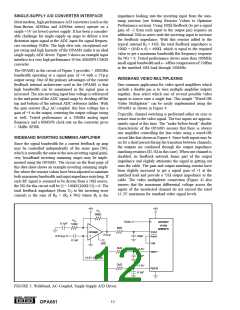
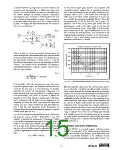
Figure 2 shows the AC-coupled, gain of +2, single supply
circuit configuration used as the basis of the +5V Specifica-
tions and Typical Performance Curves. Though not a “rail-
to-rail” design, the OPA681 requires minimal input and
output voltage headroom compared to other very wideband
current feedback op amps. It will deliver a 3Vp-p output
swing on a single +5V supply with greater than 150MHz
bandwidth. The key requirement of broadband single supply
operation is to maintain input and output signal swings
within the usable voltage ranges at both the input and the
output. The circuit of Figure 2 establishes an input midpoint
bias using a simple resistive divider from the +5V supply
(two 806Ω resistors). The input signal is then AC coupled
into this midpoint voltage bias. The input voltage can swing
to within 1.5V of either supply pin, giving a 2Vp-p input
signal range centered between the supply pins. The input
impedance matching resistor (57.6Ω) used for testing is
adjusted to give a 50Ω input match when the parallel
combination of the biasing divider network is included. The
gain resistor (RG) is AC-coupled, giving the circuit a DC
gain of +1—which puts the input DC bias voltage (2.5V) on
the output as well. The feedback resistor value has been
adjusted from the bipolar supply condition to re-optimize for
a flat frequency response in +5V, gain of +2, operation (see
Setting Resistor Values to Optimize Bandwidth). Again, on
a single +5V supply, the output voltage can swing to within
1V of either supply pin while delivering more than 80mA
output current. A demanding 100Ω load to a midpoint bias
is used in this characterization circuit. The new output stage
used in the OPA681 can deliver large bipolar output currents
into this midpoint load with minimal crossover distortion, as
shown by the +5V supply, 3rd harmonic distortion plots.
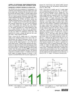
Figure 1 shows the DC coupled, gain of +2, dual power
supply circuit configuration used as the basis of the ±5V
Specifications and Typical Performance Curves. For test
purposes, the input impedance is set to 50Ω with a resistor
to ground and the output impedance is set to 50Ω with a
series output resistor. Voltage swings reported in the speci-
fications are taken directly at the input and output pins while
load powers (dBm) are defined at a matched 50Ω load. For
the circuit of Figure 1, the total effective load will be 100Ω
|| 804Ω = 89Ω. The disable control line (DIS) is typically left
open to guarantee normal amplifier operation. One optional
component is included in Figure 1. In addition to the usual
power supply de-coupling capacitors to ground, a 0.1µF
capacitor is included between the two power supply pins. In
+5V
+VS
+5V
+VS
0.1µF
6.8µF
+
+
0.1µF
6.8µF
50Ω Source
806Ω
806Ω
DIS
0.1µF
50Ω Load
DIS
VO 100Ω
VI
VO 50Ω
50Ω
OPA681
VI
57.6Ω
VS/2
OPA681
0.1µF
RF
499Ω
RF
402Ω
RG
RG
402Ω
499Ω
6.8µF
0.1µF
0.1µF
+
–VS
–5V
FIGURE 2. AC-Coupled, G = +2, Single Supply Specifica-
tion and Test Circuit.
FIGURE 1. DC-Coupled, G = +2, Bipolar Supply, Specifi-
cation and Test Circuit.
®
11
OPA681

 BB [ BURR-BROWN CORPORATION ]