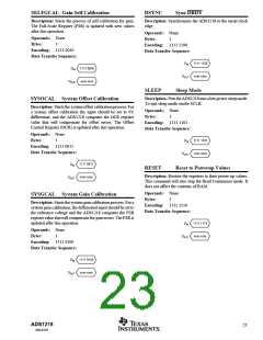
SELFGCAL Gain Self Calibration
DSYNC
Sync DRDY
Description: Starts the process of self-calibration for gain.
The Full-Scale Register (FSR) is updated with new values
after this operation.
Description: Synchronizes the ADS1218 to the serial clock
edge.
Operands: None
Operands: None
Bytes:
1
Bytes:
1
Encoding: 1111 1100
Encoding: 1111 0010
Data Transfer Sequence:
Data Transfer Sequence:
1111 1100
xxxx xxxx
DIN
1111 0010
xxxx xxxx
DIN
DOUT
DOUT
SLEEP
Sleep Mode
Description:PutstheADS1218intoalowpowersleepmode.
To exit sleep mode strobe SCLK.
SYSOCAL System Offset Calibration
Description: Starts the system offset calibration process. For
a system offset calibration the input should be set to 0V
differential, and the ADS1218 computes the OCR register
value that will compensate for offset errors. The Offset
Control Register (OCR) is updated after this operation.
Operands: None
Bytes:
1
Encoding: 1111 1101
Data Transfer Sequence:
Operands: None
Bytes:
1
DIN
1111 1101
xxxx xxxx
Encoding: 1111 0011
Data Transfer Sequence:
DOUT
1111 0011
xxxx xxxx
DIN
RESET
Reset to Powerup Values
Description: Restore the registers to their power-up values.
This command will also stop the Read Continuous mode. It
does not affect the contents of RAM.
DOUT
Operands: None
SYSGCAL System Gain Calibration
Bytes:
1
Description: Starts the system gain calibration process. For a
system gain calibration, the differential input should be set to
the reference voltage and the ADS1218 computes the FSR
register value that will compensate for gain errors. The FSR is
updated after this operation.
Encoding: 1111 1110
Data Transfer Sequence:
1111 1110
xxxx xxxx
DIN
Operands: None
Bytes:
1
DOUT
Encoding: 1111 0100
Data Transfer Sequence:
1111 0100
xxxx xxxx
DIN
DOUT
ADS1218
23
SBAS187

 BB [ BURR-BROWN CORPORATION ]