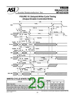
VRAM
SMJ44C251B
MT42C4256
Austin Semiconductor, Inc.
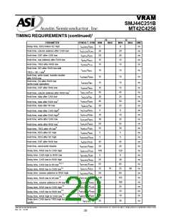
TIMING REQUIREMENTS (continued)1
-10
-12
PARAMETER
SYM/ALT. SYM MIN
MAX
MIN
MAX
UNIT
Delay time, TRG\ high before data applied at DQ
t
/t
25
30
ns
d(GHD) OED
Delay time, RAS\ low to TRG\ high
(real-time-reload read-transfer cycle only)
Delay time, RAS\ low to first SC high after
t
/t
90
95
ns
ns
d(RLTH) RTH
t
t
/t
130
40
140
d(RLSH) RSD
14
TRG\ high
Delay time, CAS\ low to first SC high after TRG\
/t
45
ns
d(CLSH) CSD
14
high
14,15,16
t
/t
15
20
ns
ns
d(SCTR) TSL
Delay time, SC high to TRG\ high
15,16
t
t
/t
-10
-10
d(THRH) TRD
Delay time, TRG\ high to RAS\ high
Delay time, SC high to RAS\ low with
/t
10
20
ns
ns
d(SCRL) SRS
6, 17, 18
TRG\ = W\ = low
Delay time, SC high to SE\ high in serial-input
mode
t
20
25
20
30
d(SCSE)
6
t
/t
ns
ns
ns
ns
d(RHSC) SRD
Delay time, RAS\ high to SC high
19
t
/t
t
t
d(THRL) TRP
w(RH)
35
w(RH)
40
Delay time, TRG\ high to RAS\ low
15, 16
t
/t
d(THSC) TSD
Delay time, TRG\ high to SC high
20
t
/t
10
15
d(SESC) SWS
Delay time, SE\ low to SC high
Delay time, RAS\ high to last (most significant)
rising edge of SC before boundary switch during
split-register read-transfer cycles
t
15
20
ns
d(RHMS)
Delay time, CAS\ low to TRG\ high in real-time
read-transfer cycles
Delay time, column address to first SC in early-
load read-transfer cycles
Delay time, column address to TRG\ high in real-
time read-transfer cycles
t
/t
5
5
ns
ns
ns
d(CLGH) CTH
t
t
/t
45
10
50
10
d(CASH) ASD
/t
d(CAGH) ATH
12
t
/t
15
0
50
15
0
60
ns
ns
ns
ns
ns
d(RLCA) RAD
Delay time, RAS\ low to column address
Delay time, data to CAS\ low
t
/t
d(DCL) DZC
Delay time, data to TRG\ low
t
/t
0
0
d(DGL) DZO
Delay time, RAS\ low to serial-input data
Delay time, TRG\ low to RAS\ high
t
/t
50
25
50
30
d(RLSD) SDD
t
/t
d(GLRH) ROH
Delay time, last (most significant) rising edge of
SC to RAS\ low before boundary switch during
split-register read-transfer cycles
Delay time, last (255 or 511) rising edge of SC to
QSF switching a the boundary during split-register
t
25
25
ns
ns
d(MSRL)
t
/t
40
40
d(SCQSF) SQD
21
read transfer cycles
Delay time, CAS\ low to QSF switching in read-
t
/t
35
30
75
35
30
75
ns
ns
ns
d(CLQSF) CQD
21
transfer or write-transfer cycles
Delay time, TRG\ high to QSF switching in read-
t
/t
d(GHQSF) TQD
21
transfer or write-transfer cycles
Delay time, RAS\ low to QSF switching in read-
t
/t
d(RLQSF) RQD
21
transfer or write-transfer cycles
Refresh time interval, memory
Transition time
t /t
8
8
ms
ns
rf REF
t /t
t
3
50
3
50
T
Austin Semiconductor, Inc. reserves the right to change products or specifications without notice.
SMJ44C251B/MT42C4256
Rev. 0.1 12/03
21

 AUSTIN [ AUSTIN SEMICONDUCTOR ]