VRAM
SMJ44C251B
MT42C4256
Austin Semiconductor, Inc.
NOTES:
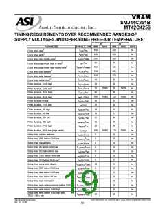
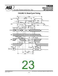
1. Timing measurements are referenced to VIL max and VIH min.
2. All cycle times assume tt = 5 ns.
3. When the odd tap is used (tap address can be 0–511, and odd taps are 1, 3, 5, etc.), the cycle time for SC in the first serial data out cycle needs to
be 70 ns minimum.
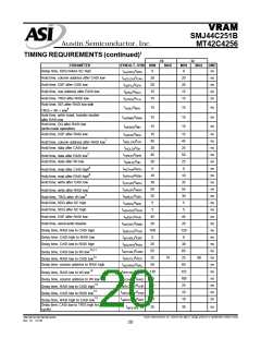
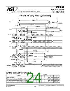
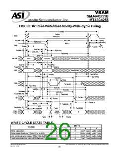
4. In a read-modify-write cycle, td(CLWL) and tsu(WCH) must be observed. Depending on the user’s transition times, this may require additional CAS\ low
time [tw(CL)].
5. In a read-modify-write cycle, td(RLWL) and tsu(WRH) must be observed. Depending on the user’s transition times, this may require additional RAS\ low
time [tw(RL)].
6. Register-to-memory (write) transfer cycles only
7. The minimum value is measured when td(RLCL) is set to td(RLCL) min as a reference.
8. Either th(RHrd) or t(CHrd) must be satisfied for a read cycle.
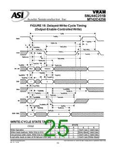
9. Output-enable-controlled write. Output remains in the high-impedance state for the entire cycle.
10. Read-modify-write operation only
11. TRG\ must disable the output buffers prior to applying data to the DQ terminals.
12. The maximum value is specified only to assure RAS\ access time.
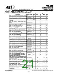
13. CAS\-before-RAS\ refresh operation only
14. Early-load read-transfer cycle only
15. Real-time-reload read-transfer cycle only
16. Late-load read-transfer cycle only
17. In a read-transfer cycle, the state of SC when RAS\ falls is a don’t care condition. However, to assure proper sequencing of the internal clock
circuitry, there can be no positive transitions of SC for at least 10 ns prior to when RAS\ goes low.
18. In a memory-to-register (read) transfer cycle, td(SCRL) applies only when the SAM was previously in serial-input mode.
19. Memory-to-register (read) and register-to-memory (write) transfer cycles only
20. Serial data-in cycles only
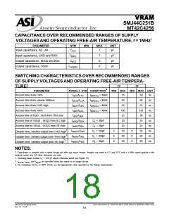
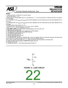
21. Switching times assume CL = 100 pF unless otherwise noted (see Figure 12).
FIGURE 12: LOAD CIRCUIT
Austin Semiconductor, Inc. reserves the right to change products or specifications without notice.
SMJ44C251B/MT42C4256
Rev. 0.1 12/03
22

 AUSTIN [ AUSTIN SEMICONDUCTOR ]